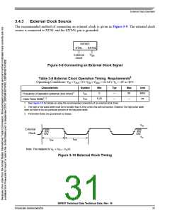
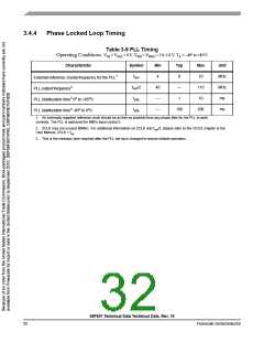
3.4.4
Phase Locked Loop Timing
Table 3-9 PLL Timing
Operating Conditions: VSS = VSSA = 0 V, VDD = VDDA = 3.0–3.6 V, TA = –40° to +85°C
Characteristic
Symbol
fosc
Min
4
Typ
8
Max
10
Unit
MHz
MHz
ms
External reference crystal frequency for the PLL1
PLL output frequency2
fout/2
tplls
40
—
—
—
110
10
PLL stabilization time3 0o to +85oC
PLL stabilization time3 -40o to 0oC
1
tplls
100
200
ms
1. An externally supplied reference clock should be as free as possible from any phase jitter for the PLL to work
correctly. The PLL is optimized for 8MHz input crystal.2.
2. ZCLK may not exceed 80MHz. For additional information on ZCLK and fout/2, please refer to the OCCS chapter in the
User Manual. ZCLK = fop
3. This is the minimum time required after the PLL set-up is changed to ensure reliable operation.
56F807 Technical Data Technical Data, Rev. 16
32
Freescale Semiconductor

 FREESCALE [ Freescale ]