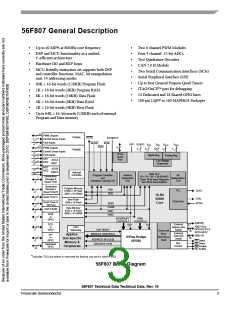
56F807 General Description
•
•
Up to 40 MIPS at 80MHz core frequency
•
•
•
•
•
•
•
•
•
•
Two 6 channel PWM Modules
DSP and MCU functionality in a unified,
C-efficient architecture
Four 4 channel, 12-bit ADCs
Two Quadrature Decoders
•
•
Hardware DO and REP loops
CAN 2.0 B Module
MCU-friendly instruction set supports both DSP
and controller functions: MAC, bit manipulation
unit, 14 addressing modes
Two Serial Communication Interfaces (SCIs)
Serial Peripheral Interface (SPI)
Up to four General Purpose Quad Timers
JTAG/OnCETM port for debugging
14 Dedicated and 18 Shared GPIO lines
160-pin LQFP or 160 MAPBGA Packages
•
•
•
•
•
•
60K × 16-bit words (120KB) Program Flash
2K × 16-bit words (4KB) Program RAM
8K × 16-bit words (16KB) Data Flash
4K × 16-bit words (8KB) Data RAM
2K × 16-bit words (4KB) Boot Flash
Up to 64K × 16- bit words (128KB) each of external
Program and Data memory
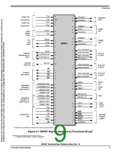
6
PWM Outputs
PWMA
PWMB
RSTO
EXTBOOT
IRQB
Current Sense Inputs
Fault Inputs
3
4
RESET
IRQA
VPP VCAPC
2
V
V
V
V
SSA
DD
SS
DDA
6
6
PWM Outputs
8
10*
3
3
Current Sense Inputs
Fault Inputs
3
4
4
4
JTAG/
OnCE
Port
Digital Reg
Analog Reg
A/D1
A/D2
ADCA
Low Voltage
Supervisor
VREF
A/D1
A/D2
ADCB
4
4
VREF2
Interrupt
Controller
Data ALU
Address
Generation
Unit
Bit
Manipulation
Unit
Program Controller
and
Hardware Looping Unit
Quadrature
Decoder 0
/Quad Timer
16 x 16 + 36 → 36-Bit MAC
Three 16-bit Input Registers
Two 36-bit Accumulators
4
Quadrature
Decoder 1
/Quad Timer B
Program Memory
61440 x 16 Flash
2048 x 16 SRAM
PAB
PLL
CLKO
4
2
•
PDB
16-Bit
56800
Core
•
•
Quad Timer C
XTAL
Boot Flash
2048 x 16 Flash
Clock Gen
Quad Timer D
/ Alt Func
EXTAL
XDB2
4
2
CGDB
Data Memory
8192 x 16 Flash
4096 x 16 SRAM
CAN 2.0A/B
•
•
•
•
XAB1
SCI0
or
GPIO
XAB2
•
INTERRUPT
CONTROLS
IPBB
CONTROLS
16
2
2
A[00:05]
SCI1
or
GPIO
External
Address Bus
Switch
16
6
A[06:15] or
GPIO-E2:E3 &
GPIO-A0:A7
COP/
Watchdog
COP RESET
External
Bus
Interface
Unit
10
16
External
Data Bus
Switch
MODULE CONTROLS
Applica-
tion-Specific
Memory &
Peripherals
SPI
or
GPIO
D[00:15]
IPBus Bridge
(IPBB)
ADDRESS BUS [8:0]
DATA BUS [15:0]
PS Select
DS Select
WR Enable
RD Enable
4
Bus
Control
Dedicated
GPIO
14
*includes TCS pin which is reserved for factory use and is tied to VSS
56F807 Block Diagram
56F807 Technical Data Technical Data, Rev. 16
Freescale Semiconductor
3

 FREESCALE [ Freescale ]