56F8036 Data Sheet Table of Contents
Part 1 Overview. . . . . . . . . . . . . . . . . . . . . . . . 5
Part 7 Security Features . . . . . . . . . . . . . . .112
1.1
1.2
1.3
56F8036 Features. . . . . . . . . . . . . . . . . . . 5
56F8036 Description. . . . . . . . . . . . . . . . . 7
Award-Winning Development
7.1
7.2
Operation with Security Enabled . . . . . 112
Flash Access Lock and Unlock
Mechanisms. . . . . . . . . . . . . . . . . 113
Product Analysis. . . . . . . . . . . . . . . . . . 114
Environment . . . . . . . . . . . . . . . . . . . 8
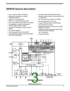
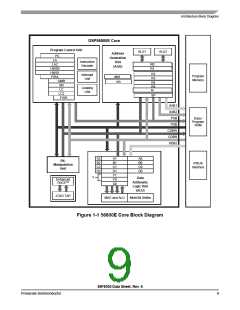
Architecture Block Diagram . . . . . . . . . . . 8
Product Documentation . . . . . . . . . . . . . 16
Data Sheet Conventions. . . . . . . . . . . . . 16
7.3
1.4
1.5
1.6
Part 8 General Purpose Input/Output
(GPIO) . . . . . . . . . . . . . . . . . . . . . . . .114
8.1
8.2
8.3
Introduction. . . . . . . . . . . . . . . . . . . . . . 114
Configuration . . . . . . . . . . . . . . . . . . . . 114
Reset Values . . . . . . . . . . . . . . . . . . . . 117
Part 2 Signal/Connection Descriptions . . . 17
2.1
2.2
Introduction . . . . . . . . . . . . . . . . . . . . . . . 17
56F8036 Signal Pins. . . . . . . . . . . . . . . . 21
Part 9 Joint Test Action Group (JTAG) . . .122
Part 3 OCCS . . . . . . . . . . . . . . . . . . . . . . . . . 33
9.1
56F8036 Information . . . . . . . . . . . . . . 122
3.1
3.2
3.3
3.4
3.5
3.6
3.7
Overview. . . . . . . . . . . . . . . . . . . . . . . . . 33
Features . . . . . . . . . . . . . . . . . . . . . . . . . 33
Operating Modes . . . . . . . . . . . . . . . . . . 33
Internal Clock Source . . . . . . . . . . . . . . . 34
Crystal Oscillator. . . . . . . . . . . . . . . . . . . 34
Ceramic Resonator. . . . . . . . . . . . . . . . . 35
External Clock Input - Crystal Oscillator
Option. . . . . . . . . . . . . . . . . . . . . . . 35
Part 10 Specifications . . . . . . . . . . . . . . . . .122
10.1
10.2
10.3
10.4
10.5
10.6
10.7
10.8
General Characteristics . . . . . . . . . . . . 122
DC Electrical Characteristics . . . . . . . . 126
AC Electrical Characteristics . . . . . . . . 129
Flash Memory Characteristics . . . . . . . 129
External Clock Operation Timing . . . . . 130
Phase Locked Loop Timing . . . . . . . . . 131
Relaxation Oscillator Timing. . . . . . . . . 131
Reset, Stop, Wait, Mode Select, and
3.8
Alternate External Clock Input . . . . . . . . 36
Part 4 Memory Maps. . . . . . . . . . . . . . . . . . . 36
Interrupt Timing . . . . . . . . . . . . . . 133
Serial Peripheral Interface (SPI)
4.1
4.2
4.3
4.4
4.5
4.6
Introduction . . . . . . . . . . . . . . . . . . . . . . . 36
Interrupt Vector Table . . . . . . . . . . . . . . . 37
Program Map . . . . . . . . . . . . . . . . . . . . . 39
Data Map . . . . . . . . . . . . . . . . . . . . . . . . 40
EOnCE Memory Map . . . . . . . . . . . . . . . 41
Peripheral Memory-Mapped Registers . . 42
10.9
Timing . . . . . . . . . . . . . . . . . . . . . 134
10.10 Quad Timer Timing. . . . . . . . . . . . . . . . 137
10.11 Serial Communication Interface (SCI)
Timing . . . . . . . . . . . . . . . . . . . . . 138
10.12 Freescale’s Scalable Controller Area
Network (MSCAN) Timing . . . . . . 139
10.13 Inter-Integrated Circuit Interface (I2C)
Timing . . . . . . . . . . . . . . . . . . . . . 139
10.14 JTAG Timing. . . . . . . . . . . . . . . . . . . . . 141
10.15 Analog-to-Digital Converter (ADC)
Parameters . . . . . . . . . . . . . . . . . 142
Part 5 Interrupt Controller (ITCN) . . . . . . . . 56
5.1
5.2
5.3
5.4
5.5
5.6
5.7
Introduction . . . . . . . . . . . . . . . . . . . . . . . 56
Features . . . . . . . . . . . . . . . . . . . . . . . . . 56
Functional Description . . . . . . . . . . . . . . 56
Block Diagram. . . . . . . . . . . . . . . . . . . . . 58
Operating Modes . . . . . . . . . . . . . . . . . . 59
Register Descriptions . . . . . . . . . . . . . . . 59
Resets. . . . . . . . . . . . . . . . . . . . . . . . . . . 78
10.16 Equivalent Circuit for ADC Inputs. . . . . 143
10.17 Comparator (CMP) Parameters . . . . . . 143
10.18 Digital-to-Analog Converter (DAC)
Parameters . . . . . . . . . . . . . . . . . 144
Part 6 System Integration Module (SIM). . . 79
10.19 Power Consumption . . . . . . . . . . . . . . . 145
6.1
6.2
6.3
6.4
6.5
6.6
6.7
6.8
Introduction . . . . . . . . . . . . . . . . . . . . . . . 79
Features . . . . . . . . . . . . . . . . . . . . . . . . . 79
Register Descriptions . . . . . . . . . . . . . . . 81
Clock Generation Overview . . . . . . . . . 107
Power-Saving Modes . . . . . . . . . . . . . . 108
Resets. . . . . . . . . . . . . . . . . . . . . . . . . . 109
Clocks . . . . . . . . . . . . . . . . . . . . . . . . . . 110
Interrupts. . . . . . . . . . . . . . . . . . . . . . . . 112
Part 11 Packaging . . . . . . . . . . . . . . . . . . . .147
11.1
56F8036 Package and Pin-Out
Information. . . . . . . . . . . . . . . . . . 147
Part 12 Design Considerations. . . . . . . . . .150
12.1
12.2
Thermal Design Considerations . . . . . . 150
Electrical Design Considerations . . . . . 151
Part 13 Ordering Information . . . . . . . . . . .152
Part 14 Appendix . . . . . . . . . . . . . . . . . . . . .153
56F8036 Data Sheet, Rev. 6
4
FreescaleSemiconductor

 FREESCALE [ Freescale ]