development of optimized control applications.
The 56F8036 supports program execution from internal memories. Two data operands can be accessed
from the on-chip data RAM per instruction cycle. The 56F8036 also offers up to 39 General Purpose
Input/Output (GPIO) lines, depending on peripheral configuration.
The 56F8036 Digital Signal Controller includes 64KB of Program Flash and 8KB of Unified
Data/Program RAM. Program Flash memory can be independently bulk erased or erased in pages.
Program Flash page erase size is 512 Bytes (256 Words).
A full set of programmable peripherals—PWM, ADCs, QSCI, QSPI, I2C, PITs, Quad Timers, DACs, and
analog comparators—supports various applications. Each peripheral can be independently shut down to
save power. Any pin in these peripherals can also be used as General Purpose Input/Outputs (GPIOs).
1.3 Award-Winning Development Environment
TM
Processor Expert
(PE) provides a Rapid Application Design (RAD) tool that combines easy-to-use
component-based software application creation with an expert knowledge system.
The CodeWarrior Integrated Development Environment is a sophisticated tool for code navigation,
compiling, and debugging. A complete set of evaluation modules (EVMs), demonstration board kit and
development system cards will support concurrent engineering. Together, PE, CodeWarrior and EVMs
create a complete, scalable tools solution for easy, fast, and efficient development.
1.4 Architecture Block Diagram
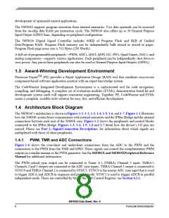
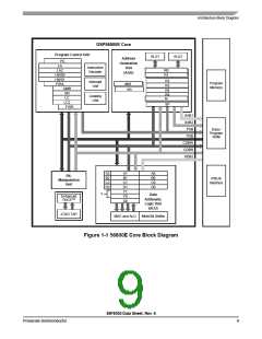
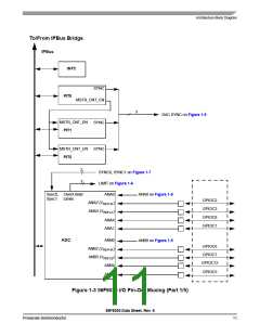
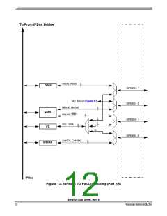
The 56F8036’s architecture is shown in Figures 1-1, 1-2, 1-3, 1-4, 1-5, 1-6, and 1-7. Figure 1-1 illustrates
how the 56800E system buses communicate with internal memories and the IPBus Bridge and the internal
connections between each unit of the 56800E core. Figure 1-2 shows the peripherals and control blocks
connected to the IPBus Bridge. Figures 1-3, 1-4, 1-5, 1-6 and 1-7 detail how the device’s I/O pins are
muxed. Please see Part 2, Signal/Connection Descriptions, for information about which signals are
multiplexed with those of other peripherals.
1.4.1
PWM, TMR and ADC Connections
Figure 1-6 shows the over-limit and under-limit connections from the ADC to the PWM and the
connections to the PWM from the TMR and GPIO. These signals can control the complementary PWM
outputs in a similar manner as the PWM generator. See the 56F802X and 56F803XPeripheral Reference
Manual for additional information.
The PWM_reload_sync output can be connected to Timer A’s (TMRA) Channel 3 input; TMRA’s
Channels 2 and 3 outputs are connected to the ADC sync inputs. TMRA Channel 3 output is connected to
SYNC0 and TMRA Channel 2 is connected to SYNC1. SYNC0 is the master ADC sync input that is used
to trigger ADCA and ADCB in sequence and parallel mode. SYNC1 is used to trigger ADCB in parallel
independent mode. These are controlled by bits in the SIM Control Register; see Section 6.3.1.
56F8036 Data Sheet, Rev. 6
8
FreescaleSemiconductor

 FREESCALE [ Freescale ]