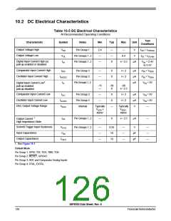
Table 10-9 Flash Timing Parameters
Characteristic
Symbol
Tprog
Terase
Tme
Min
20
Typ
—
Max
40
Unit
μs
Program time1
Erase time 2
20
—
—
ms
ms
Mass erase time
100
—
—
1. There is additional overhead which is part of the programming sequence. See the 56F802X and 56F803XPeripheral
Reference Manual for details.
2. Specifies page erase time. There are 512 bytes per page in the Program Flash memory.
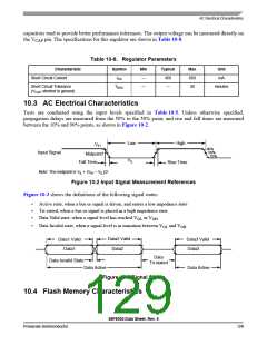
10.5 External Clock Operation Timing
1
Table 10-10 External Clock Operation Timing Requirements
Characteristic
Symbol
fosc
Min
4
Typ
8
Max
8
Unit
MHz
ns
Frequency of operation (external clock driver)2
Clock Pulse Width3
tPW
6.25
—
—
—
—
—
3
External Clock Input Rise Time4
trise
ns
External Clock Input Fall Time5
tfall
—
3
ns
1. Parameters listed are guaranteed by design.
2. See Figure 10-4 for details on using the recommended connection of an external clock driver.
3. The chip may not function if the high or low pulse width is smaller than 6.25ns.
4. External clock input rise time is measured from 10% to 90%.
5. External clock input fall time is measured from 90% to 10%.
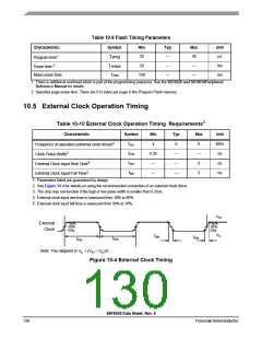
VIH
External
Clock
90%
50%
10%
90%
50%
10%
VIL
tfall
trise
tPW
tPW
Note: The midpoint is VIL + (VIH – VIL)/2.
Figure 10-4 External Clock Timing
56F8036 Data Sheet, Rev. 6
130
FreescaleSemiconductor

 FREESCALE [ Freescale ]