Reset Values
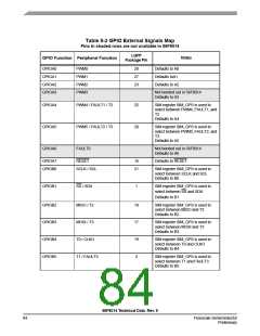
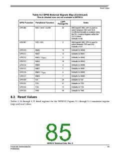
Table 8-2 GPIO External Signals Map (Continued)
Pins in shaded rows are not available in 56F8014
LQFP
Package Pin
Notes
GPIO Function Peripheral Function
GPIOB6
RXD / SDA / CLKIN
32
SIM register SIM_GPS is used to
select between RXD and SDA.
CLKIN functionality is enabled using
the PLL Control Register within the
OCCS block.
Defaults to B6
GPIOB7
TXD / SCL
2
SIM register SIM_GPS is used to
select between TXD and SCL
Defaults to B7
GPIOC0
GPIOC1
GPIOC2
ANA0
13
12
11
Defaults to ANA0
Defaults to ANA1
Defaults to ANA2
ANA1
ANA2 / VREFH
GPIOC3
GPIOC4
GPIOC5
GPIOC6
ANA3
10
4
Defaults to ANA3
Defaults to ANB0
Defaults to ANB1
Defaults to ANB2
ANB0
ANB1
5
ANB2 / VREFL
6
GPIOC7
GPIOD0
GPIOD1
GPIOD2
GPIOD3
ANB3
TDI
7
Defaults to ANB3
Defaults to TDI
Defaults to TDO
Defaults to TCK
Defaults to TMS
29
31
15
30
TDO
TCK
TMS
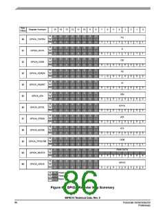
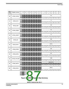
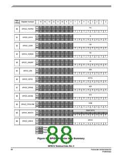
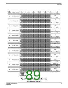
8.3 Reset Values
Tables 4-16 through 4-19 detail registers for the 56F8014; Figures 8-1 through 8-4 summarize register
maps and reset values.
56F8014 Technical Data, Rev. 9
Freescale Semiconductor
Preliminary
85

 FREESCALE [ Freescale ]