Electrical Characteristics
2.1.2
Power Supply Voltage Specification
Table 2 provides the recommended operating conditions for the MPC8349EA. Note that the values in
Table 2 are the recommended and tested operating conditions. Proper device operation outside these
conditions is not guaranteed.
Table 2. Recommended Operating Conditions
Recommended
Parameter
Symbol
Unit
Notes
Value
Core supply voltage for 667-MHz core frequency
Core supply voltage
VDD
VDD
1.3 V 60 mV
1.2 V 60 mV
1.3 V 60 mV
1.2 V 60 mV
V
V
V
V
V
1
1
PLL supply voltage for 667-MHz core frequency
PLL supply voltage
AVDD
AVDD
GVDD
1
1
DDR and DDR2 DRAM I/O voltage
2.5 V 125 mV
1.8 V 90 mV
—
Three-speed Ethernet I/O supply voltage
Three-speed Ethernet I/O supply voltage
LVDD1
LVDD2
OVDD
3.3 V 330 mV
2.5 V 125 mV
V
V
V
—
—
—
3.3 V 330 mV
2.5 V 125 mV
PCI, local bus, DUART, system control and power
management, I2C, and JTAG I/O voltage
3.3 V 330 mV
Note:
1
GVDD, LVDD, OVDD, AVDD, and VDD must track each other and must vary in the same direction—either in the positive or
negative direction.
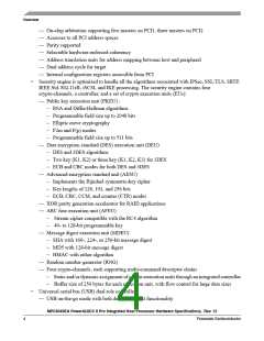
Figure 2 shows the undershoot and overshoot voltages at the interfaces of the MPC8349EA.
G/L/OVDD + 20%
G/L/OVDD + 5%
G/L/OVDD
VIH
GND
GND – 0.3 V
VIL
GND – 0.7 V
Not to Exceed 10%
1
of tinterface
Note:
1. tinterface refers to the clock period associated with the bus clock interface.
Figure 2. Overshoot/Undershoot Voltage for GV /OV /LV
DD
DD
DD
MPC8349EA PowerQUICC II Pro Integrated Host Processor Hardware Specifications, Rev. 13
Freescale Semiconductor
8

 FREESCALE [ Freescale ]