Electrical Characteristics (TA = 25°C unless otherwise noted)
Symbol Parameter Conditions
DRAIN-SOURCE DIODE CHARACTERISTICS AND MAXIMUM RATINGS
Min
Typ
Max
Units
IS
Maximum Continuos Drain-Source Diode Forward Current
1.8
1.2
A
V
Drain-Source Diode Forward Voltage
Reverse Recovery Time
0.84
VSD
trr
VGS = 0 V, IS = 1.25 A (Note 2)
VGS = 0V, IF = 1.25 A, dIF/dt = 100 A/µs
100
ns
Notes:
1. RqJA is the sum of the junction-to-case and case-to-ambient thermal resistance where the case thermal reference is defined as the solder mounting surface of the drain pins. RqJC is guaranteed by
design while RqCA is determined by the user's board design.
T - T
T - T
=
=
(t)
R
qJ
= I2 (t) ´ RDS
J
A
J
A
( )
PD t
(
)
T
J
ON
D
R
+R (t)
C qCA
qJ
A
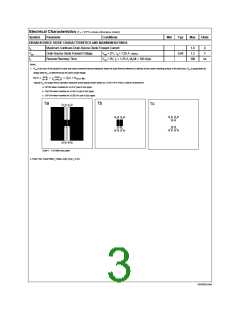
Typical RqJA for single device operation using the board layouts shown below on 4.5"x5" FR-4 PCB in a still air environment:
a. 78oC/W when mounted on a 0.5 in2 pad of 2oz cpper.
b. 125oC/W when mounted on a 0.02 in2 pad of 2oz cpper.
c. 135oC/W when mounted on a 0.003 in2 pad of 2oz cpper.
1a
1b
1c
Scale 1 : 1 on letter size paper
2. Pulse Test: Pulse Width < 300µs, Duty Cycle < 2.0%.
NDS9959.SAM

 FAIRCHILD [ FAIRCHILD SEMICONDUCTOR ]