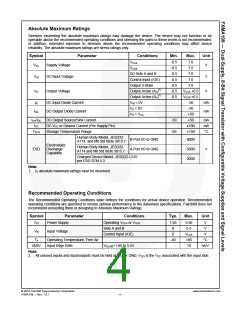
Absolute Maximum Ratings
Stresses exceeding the absolute maximum ratings may damage the device. The device may not function or be
operable above the recommended operating conditions and stressing the parts to these levels is not recommended.
In addition, extended exposure to stresses above the recommended operating conditions may affect device
reliability. The absolute maximum ratings are stress ratings only.
Symbol
Parameter
Conditions
Min.
-0.5
-0.5
-0.5
-0.5
-0.5
-0.5
-0.5
Max.
7.0
Unit
VCCA
VCCB
VCC
Supply Voltage
V
7.0
I/O Side A and B
Control Input (/OE)
Output 3-State
Output Active (An)(1)
Output Active (Bn)(1)
VIN < 0V
7.0
VIN
VO
DC Input Voltage
V
V
7.0
7.0
Output Voltage
VCCA +0.5
VCCB +0.5
-50
IIK
DC Input Diode Current
DC Output Diode Current
mA
mA
VO < 0V
-50
IOK
VO > VCC
+50
IOH/IOL
ICC
DC Output Source/Sink Current
DC VCC or Ground Current (Per Supply Pin)
Storage Temperature Range
-50
-65
+50
mA
mA
°C
±100
+150
TSTG
Human Body Model, JESD22-
A114, and Mil Std 883e 3015.7
B Port I/O to GND
A Port I/O to GND
8000
5000
2000
Electrostatic
Human Body Model, JESD22-
Discharge
ESD
V
A114 and Mil Std 883e 3015.7
Capability
Charged Device Model, JESD22-C101
per ESD STM 5.3
Note:
1. IO absolute maximum ratings must be observed.
Recommended Operating Conditions
The Recommended Operating Conditions table defines the conditions for actual device operation. Recommended
operating conditions are specified to ensure optimal performance to the datasheet specifications. Fairchild does not
recommend exceeding them or designing to Absolute Maximum Ratings.
Symbol
Parameter
Power Supply
Conditions
Operating VCCA or VCCB
Side A and B
Typ.
1.65
0
Max.
5.50
5.5
Unit
V
VCC
V
VIN
Input Voltage
Control Input (/OE)
0
VCCA
+85
10
V
TA
dt/dV
Operating Temperature, Free Air
Input Edge Rate
-40
°C
ns/V
VCCA/B=1.65 to 5.5V
Note:
2. All unused inputs and input/outputs must be held at VCCI or GND. VCCI is the VCC associated with the input side.
© 2010 Fairchild Semiconductor Corporation
FXMA108 • Rev. 1.0.1
www.fairchildsemi.com
4

 FAIRCHILD [ FAIRCHILD SEMICONDUCTOR ]