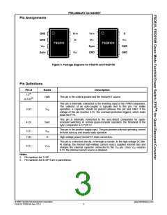
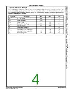
PRELIMINARY DATASHEET
Functional Description
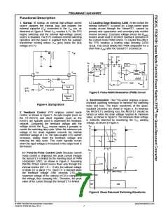
1. Startup: At startup, an internal high-voltage current
source supplies the internal bias and charges the
external capacitor (Ca) connected to the VCC pin, as
illustrated in Figure 4. When VCC reaches 8.7V, the FPS
begins switching and the internal high-voltage current
source is disabled. The FPS continues normal switching
operation and the power is supplied from the auxiliary
transformer winding unless VCC goes below the stop
voltage of 6.7V.
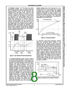
2.2 Leading Edge Blanking (LEB): At the instant the
internal SenseFET is turned on, a high-current spike
usually occurs through the SenseFET, caused by
primary-side capacitance and secondary-side rectifier
reverse recovery. Excessive voltage across the Rsense
resistor would lead to incorrect feedback operation in
the current mode PWM control. To counter this effect,
the FPS employs a leading edge blanking (LEB)
circuit. This circuit inhibits the PWM comparator for a
short time (tLEB) after the SenseFET is turned on.
VDC
Vcc
Idelay
Vref
IFB
Ca
Vfb
Vo
SenseFET
OSC
3
H11A817A
D1
D2
CB
6R
R
+
Gate
driver
Vcc
VSTR
Vfb*
5
8
KA431
-
ICH
OLP
Rsense
VSD
Vref
6.7V/
8.7V
Vcc good
Figure 5. Pulse-Width Modulation (PWM) Circuit
Internal
Bias
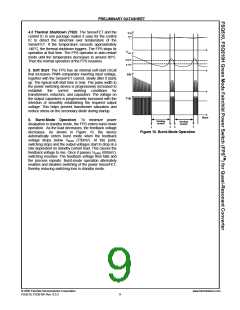
3. Synchronization: The FSQ-series employs a quasi-
resonant switching technique to minimize the switching
noise and loss. The basic waveforms of the quasi-
resonant converter are shown in Figure 6. To minimize
the MOSFET's switching loss, the MOSFET should be
turned on when the drain voltage reaches its minimum
value, as shown in Figure 6. The minimum drain voltage
is indirectly detected by monitoring the VCC winding
voltage, as shown in Figure 6.
Figure 4. Startup Block
2. Feedback Control: FPS employs current mode
control, as shown in Figure 5. An opto-coupler (such as
the H11A817A) and shunt regulator (such as the
KA431) are typically used to implement the feedback
network. Comparing the feedback voltage with the
voltage across the Rsense resistor makes it possible to
control the switching duty cycle. When the reference pin
voltage of the shunt regulator exceeds the internal
reference voltage of 2.5V, the opto-coupler LED current
increases, pulling down the feedback voltage and
reducing the duty cycle. This event typically occurs
when the input voltage is increased or the output load is
decreased.
VDS
VRO
VRO
VDC
TF
VSync
2.1 Pulse-by-Pulse Current Limit: Because current
mode control is employed, the peak current through
the SenseFET is limited by the inverting input of PWM
comparator (Vfb*), as shown in Figure 5. Assuming
that the 225µA current source flows only through the
internal resistor (6R + R = 11 kΩ), the cathode voltage
of diode D2 is about 2.5V. Since D1 is blocked when
the feedback voltage (Vfb) exceeds 2.5V, the
maximum voltage of the cathode of D2 is clamped at
this voltage, thus clamping Vfb*. Therefore, the peak
value of the current through the SenseFET is limited.
0.7V
0.1V
200ns Delay
MOSFET Gate
ON
ON
Figure 6. Quasi-Resonant Switching Waveforms
© 2006 Fairchild Semiconductor Corporation
FSQ510, FSQ510H Rev. 0.0.3
www.fairchildsemi.com
7

 FAIRCHILD [ FAIRCHILD SEMICONDUCTOR ]