PRELIMINARY DATASHEET
Application Information
Application
Output Power
Input Voltage
Output Voltage (Max Current)
Cellular Phone Charger
3.3W
Universal Input (85-265Vac)
5.1V (650mA)
Features
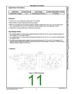
Low-cost, no Y-cap, cellular phone charger with CC/CV function
Meets CISPR-22 Class-B requirement at full-load condition
Meets CEC & Energy Star EPS program (arithmetic average of efficiencies at 25%, 50%, 75%, and 100% of full
load – measured at the end of 0.2Ω /1.5m load line, enclosed in plastic case, room temperature, still air)
Extremely low no-load standby power (<60mW at universal input)
Key Design Notes
The constant voltage (CV) mode control is implemented with resistors R2, R4, R5, and R6; feedback capacitor C8;
shunt regulator of U1; and opto-coupler U3.
The constant current (CC) mode control is designed with resistors R2, R4, R10, R11, R13, and R14; NPN transistor
Q1; and NTC THR1.
The divided bias winding voltage is applied to the sync pin with resistor R12, R15, and R16. The capacitor C9 is
added to delay the divided bias winding for switching at the minimum drain voltage. The diode D7 is used to avoid a
significant negative voltage on the sync pin.
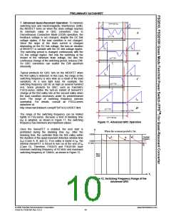
1. Schematic
Figure 13. FSQ510 Schematic
© 2006 Fairchild Semiconductor Corporation
FSQ510, FSQ510H Rev. 0.0.3
www.fairchildsemi.com
11

 FAIRCHILD [ FAIRCHILD SEMICONDUCTOR ]