PRELIMINARY DATASHEET
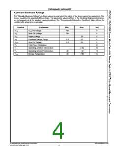
Pin Assignments
GND
GND
VFB
VSTR
D
VSTR
VFB
D
VCC
FSQ510
FSQ510H
Sync
GND
GND
GND
Sync
VCC
Figure 3. Package diagrams for FSQ510 and FSQ510H
Pin Definitions
Pin #
1,2(5)
(4,5,6)(6)
Name
Description
GND
This pin is the control ground and the SenseFET source.
This pin is internally connected to the inverting input of the PWM comparator.
The collector of an opto-coupler is typically tied to this pin. For stable
operation, a capacitor should be placed between this pin and GND. If the
voltage of this pin reaches 4.5V, the overload protection triggers, which shuts
down the FPS.
3 (2)
4 (3)
VFB
This pin is internally connected to the sync-detect comparator for quasi-
resonant switching. In normal quasi-resonant operation, the threshold of the
sync comparator is 0.7V/0.1V.
Sync
This pin is the positive supply input. This pin provides internal operating current
for both start-up and steady-state operation.
5 (7)
7 (8)
VCC
D
High-voltage power SenseFET drain connection.
This pin is connected directly, or through a resistor, to the high-voltage DC link.
At startup, the internal high-voltage current source supplies internal bias and
charges the external capacitor connected to the VCC pin. Once VCC reaches
8.7V, the internal current source is disabled.
8 (1)
VSTR
Notes:
5. Pin numbers for 7-DIP.
6. Pin numbers for 8-DIPH are in parenthesis.
© 2006 Fairchild Semiconductor Corporation
FSQ510, FSQ510H Rev. 0.0.3
www.fairchildsemi.com
3

 FAIRCHILD [ FAIRCHILD SEMICONDUCTOR ]