FSCQ-SERIES
preset maximum current to be supplied to the SMPS until the
over load protection triggers. Because more energy than
required is provided to the output, the output voltage may
exceed the rated voltage before the over load protection
triggers, resulting in the breakdown of the devices in the
secondary side. In order to prevent this situation, an over
voltage protection (OVP) circuit is employed. In general, the
peak voltage of the sync signal is proportional to the output
voltage and the FSCQ-Series uses a sync signal instead of
directly monitoring the output voltage. If the sync signal
exceeds 12V, an OVP is triggered resulting in a shutdown of
SMPS. In order to avoid undesired triggering of OVP during
normal operation, the peak voltage of the sync signal should
be designed to be below 12V. This protection is implemented
in the auto restart mode.
In the standby mode, the picture ON signal is disabled and
the transistor Q is turned off, which couples R , Dz, and D
1
1
3
to the reference pin of KA431. Then, Vo2 is determined by
the zener diode breakdown voltage. Assuming that the
forward voltage drop of D is 0.7V, V in standby mode is
o2
1
approximately given by
stby
Vo2
= VZ + 0.7 + 2.5
VO2
Micom
Linear
Regulator
VO1 (B+)
RD
Dz
Rbias
R3
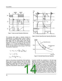
4.4 Thermal Shutdown (TSD) : The SenseFET and the
control IC are built in one package. This makes it easy for
the control IC to detect abnormal over temperature of the
SenseFET. When the temperature exceeds approximately
150°C, the thermal shutdown triggers. This protection is
implemented in the latch mode.
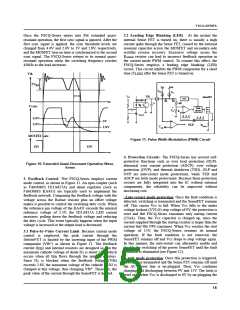
R1
D1
CF RF
Q1
Picture ON
C
A
R
KA431
R2
Figure 15. Typical Feedback Circuit to Drop Output Volt-
age in Standby Mode
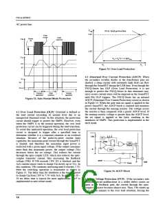
5. Soft Start : The FSCQ-Series has an internal soft-start
circuit that increases PWM comparator’s inverting input
voltage together with the SenseFET current slowly after it
starts up. The typical soft start time is 20msec. The pulse
width to the power switching device is progressively
increased to establish the correct working conditions for
transformers, inductors, and capacitors. Increasing the pulse
width to the power switching device also helps prevent
transformer saturation and reduces the stress on the
secondary diode during startup. For a fast build up of the
output voltage, an offset is introduced in the soft-start
reference current.
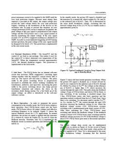
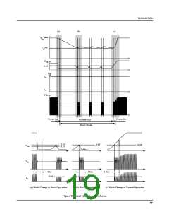
Figure 17 shows the burst mode operation waveforms. When
the picture ON signal is disabled, Q is turned off and R
1
3
and Dz are connected to the reference pin of KA431 through
D . Before V drops to V stby, the voltage on the reference
1
o2
o2
pin of KA431 is higher than 2.5V, which increases the
current through the opto LED. This pulls down the feedback
voltage (V ) of FSCQ-Series and forces FSCQ-Series to
FB
stop switching. If the switching is disabled longer than
1.4ms, FSCQ-Series enters into burst operation and the
operating current is reduced from IOP to 0.25mA (IOB). Since
stby
there is no switching, V decreases until it reaches V
o2 o2
.
As V reaches V stby, the current through the opto LED
o2 o2
6. Burst Operation : In order to minimize the power
consumption in the standby mode, the FSCQ-Series employs
burst operation. Once FSCQ-Series enters into the burst
mode, FSCQ-Series allows all output voltages and effective
switching frequency to be reduced. Figure 15 shows the
typical feedback circuit for C-TV applications. In normal
operation, the picture on signal is applied and the transistor
decreases allowing the feedback voltage to rise. When the
feedback voltage reaches 0.4V, FSCQ-Series resumes
switching with a predetermined peak drain current of 0.9A.
After burst switching for 1.4ms, FSCQ-Series stops
switching and checks the feedback voltage. If the feedback
voltage is below 0.4V, FSCQ-Series stops switching until the
feedback voltage increases to 0.4V. If the feedback voltage is
above 0.4V, FSCQ-Series goes back to the normal operation.
Q is turned on, which de-couples R , D and D1 from the
1
3
z
feedback network. Therefore, only V is regulated by the
o1
feedback circuit in normal operation and determined by R
1
and R as
2
The output voltage drop circuit can be implemented
alternatively as shown in Figure 16. In the circuit of Figure
16, the FSCQ-Series goes into burst mode, when picture off
signal is applied to Q1. Then, Vo2 is determined by the zener
diode breakdown voltage. Assuming that the forward
R1 + R2
--------------------
R2
norm
⎛
⎝
⎞
⎠
Vo1
= 2.5 ⋅
17

 FAIRCHILD [ FAIRCHILD SEMICONDUCTOR ]