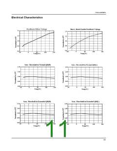
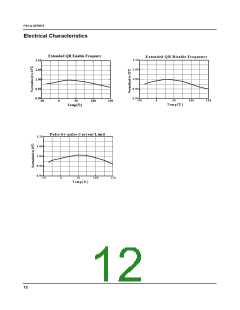
FSCQ-SERIES
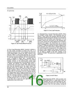
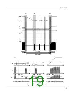
Once the FSCQ-Series enters into the extended quasi-
resonant operation, the first sync signal is ignored. After the
first sync signal is applied, the sync threshold levels are
changed from 4.6V and 2.6V to 3V and 1.8V, respectively,
and the MOSFET turn-on time is synchronized to the second
sync signal. The FSCQ-Series returns to its normal quasi-
resonant operation when the switching frequency reaches
45kHz as the load increases.
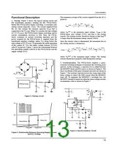
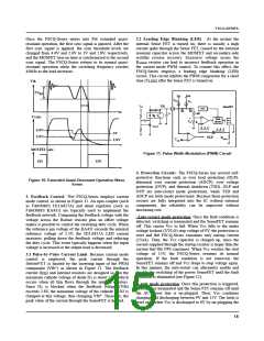
3.2 Leading Edge Blanking (LEB) : At the instant the
internal Sense FET is turned on, there is usually a high
current spike through the Sense FET, caused by the external
resonant capacitor across the MOSFET and secondary-side
rectifier reverse recovery. Excessive voltage across the
R
resistor can lead to incorrect feedback operation in
sense
the current mode PWM control. To counter this effect, the
FSCQ-Series employs a leading edge blanking (LEB)
circuit. This circuit inhibits the PWM comparator for a short
time (T
) after the Sense FET is turned on.
LEB
Vds
2VRO
Vcc
Idelay
Vref
IFB
Vfb
Vo
SenseFET
OSC
4
H11A817A
D1
D2
CB
2.5R
R
Vsync
+
Vfb*
Gate
driver
KA431
-
4.6V
2.6V
3V
1.8V
OLP
Rsense
VSD
MOSFET Gate
Figure 11. Pulse Width Modulation (PWM) Circuit
ON
ON
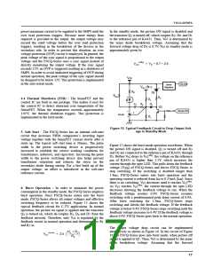
4. Protection Circuits: The FSCQ-Series has several self-
protective functions such as over load protection (OLP),
abnormal over current protection (AOCP), over voltage
protection (OVP), and thermal shutdown (TSD). OLP and
OVP are auto-restart mode protections, while TSD and
AOCP are latch mode protections. Because these protection
circuits are fully integrated into the IC without external
components, the reliability can be improved without
increasing cost.
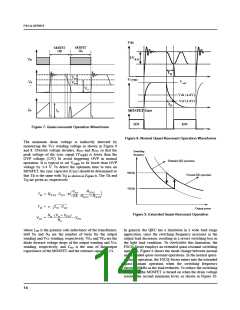
Figure 10. Extended Quasi-Resonant Operation Wave-
forms
3. Feedback Control: The FSCQ-Series employs current
mode control, as shown in Figure 11. An opto-coupler (such
as Fairchild’s H11A817A) and shunt regulator (such as
Fairchild’s KA431) are typically used to implement the
feedback network. Comparing the feedback voltage with the
voltage across the Rsense resistor plus an offset voltage
makes it possible to control the switching duty cycle. When
the reference pin voltage of the KA431 exceeds the internal
reference voltage of 2.5V, the H11A817A LED current
increases, pulling down the feedback voltage and reducing
the duty cycle. This event typically happens when the input
voltage is increased or the output load is decreased.
-Auto-restart mode protection: Once the fault condition is
detected, switching is terminated and the SenseFET remains
off. This causes Vcc to fall. When Vcc falls to the under
voltage lockout (UVLO) stop voltage of 9V, the protection is
reset and the FSCQ-Series consumes only startup current
(25uA). Then, the Vcc capacitor is charged up, since the
current supplied through the startup resistor is larger than the
current that the FPS consumes. When Vcc reaches the start
voltage of 15V, the FSCQ-Series resumes its normal
operation. If the fault condition is not removed, the
SenseFET remains off and Vcc drops to stop voltage again.
In this manner, the auto-restart can alternately enable and
disable the switching of the power SenseFET until the fault
condition is eliminated (see Figure 12).
3.1 Pulse-by-Pulse Current Limit: Because current mode
control is employed, the peak current through the
SenseFET is limited by the inverting input of the PWM
comparator (Vfb*) as shown in Figure 11. The feedback
current (I ) and internal resistors are designed so that the
FB
maximum cathode voltage of diode D is about 2.8V, which
2
occurs when all I
FB
Since D is blocked when the feedback voltage (Vfb)
1
exceeds 2.8V, the maximum voltage of the cathode of D2 is
clamped at this voltage, thus clamping Vfb*. Therefore, the
peak value of the current through the SenseFET is limited.
flows through the internal resistors.
-Latch mode protection: Once this protection is triggered,
switching is terminated and the Sense FET remains off until
the AC power line is un-plugged. Then, Vcc continues
charging and discharging between 9V and 15V. The latch is
reset only when Vcc is discharged to 6V by un-plugging the
15

 FAIRCHILD [ FAIRCHILD SEMICONDUCTOR ]