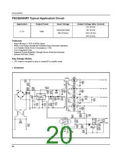
FSCQ-SERIES
AC power line.
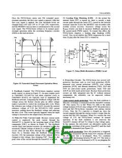
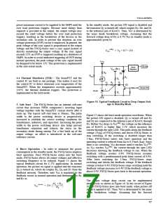
VFB
Over load protection
7.5V
Fault
occurs
Fault
removed
Power
Vds
on
2.8V
Vcc
T12= CB*(7.5-2.8)/Idelay
15V
9V
T1
Figure 13. Over Load Protection
T2
t
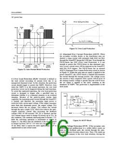
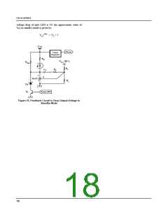
4.2 Abnormal Over Current Protection (AOCP): When
the secondary rectifier diodes or the transformer pins are
shorted, a steep current with extremely high di/dt can flow
through the SenseFET during the LEB time. Even though the
FSCQ-Series has OLP (Over Load Protection), it is not
enough to protect the FSCQ-Series in that abnormal case,
since severe current stress will be imposed on the SenseFET
until the OLP triggers. The FSCQ-Series has an internal
AOCP (Abnormal Over Current Protection) circuit as shown
in Figure 14. When the gate turn-on signal is applied to the
power SenseFET, the AOCP block is enabled and monitors
the current through the sensing resistor. The voltage across
the resistor is then compared with a preset AOCP level. If
the sensing resistor voltage is greater than the AOCP level,
the set signal is applied to the latch, resulting in the
shutdown of SMPS. This protection is implemented in the
latch mode.
ICC
IOP
ISTART
t
Normal
operation
Fault
situation
Normal
operation
Figure 12. Auto Restart Mode Protection
4.1 Over Load Protection (OLP): Overload is defined as
the load current exceeding its normal level due to an
unexpected abnormal event. In this situation, the protection
circuit should trigger to protect the SMPS. However, even
when the SMPS is in the normal operation, the over load
protection circuit can be triggered during the load transition.
To avoid this undesired operation, the over load protection
circuit is designed to trigger after a specified time to
determine whether it is a transient situation or an overload
situation. Because of the pulse-by-pulse current limit
capability, the maximum peak current through the SenseFET
is limited, and therefore the maximum input power is
restricted with a given input voltage. If the output consumes
more than this maximum power, the output voltage (Vo)
decreases below the set voltage. This reduces the current
through the opto-coupler LED, which also reduces the opto-
coupler transistor current, thus increasing the feedback
voltage (Vfb). If Vfb exceeds 2.8V, D1 is blocked, and the
2.5R
OSC
S
Q
Q
PWM
Gate
Driver
R
R
LEB
Rsense
+
-
2
AOCP
GND
Vaocp
5uA current source starts to charge C slowly up to Vcc. In
B
this condition, Vfb continues increasing until it reaches 7.5V,
then the switching operation is terminated as shown in
Figure 13. The delay time for shutdown is the time required
Figure 14. AOCP Block
to charge C from 2.8V to 7.5V with 5uA. In general, a 20 ~
B
50 ms delay time is typical for most applications. OLP is
implemented in auto restart mode.
4.3 Over Voltage Protection (OVP) : If the secondary side
feedback circuit malfunctions or a solder defect causes an
open in the feedback path, the current through the opto-
coupler transistor becomes almost zero. Then, Vfb climbs up
in a similar manner to the over load situation, forcing the
16

 FAIRCHILD [ FAIRCHILD SEMICONDUCTOR ]