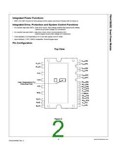
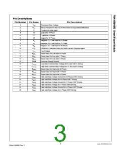
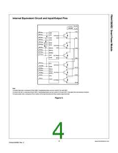
Pin Descriptions
Pin Number
Pin Name
Pin Description
1
2
VTH
RTH
Thermistor Bias Voltage
Series Resistor for the Use of Thermistor (Temperature Detection)
Positive DC–Link Input
3
P
4
U
Output for U Phase
5
V
Output for V Phase
6
W
Output for W Phase
7
NU
Negative DC–Link Input for U Phase
Negative DC–Link Input for V Phase
8
NV
9
NW
Negative DC–Link Input for W Phase
Capacitor (Low-pass Filter) for Short-Current Detection Input
Fault Output
10
11
12
13
14
15
16
17
18
19
20
21
22
23
24
25
26
CSC
VFO
IN(WL)
IN(VL)
IN(UL)
COM
VCC(L)
VCC(H)
IN(WH)
IN(VH)
IN(UH)
VS(W)
VB(W)
VS(V)
VB(V)
VS(U)
VB(U)
Signal Input for Low-side W Phase
Signal Input for Low-side V Phase
Signal Input for Low-side U Phase
Common Supply Ground
Low-Side Common Bias Voltage for IC and IGBTs Driving
High-Side Common Bias Voltage for IC and IGBTs Driving
Signal Input for High-side W Phase
Signal Input for High-side V Phase
Signal Input for High-side U Phase
High-side Bias Voltage Ground for W Phase IGBT Driving
High-side Bias Voltage for W Phase IGBT Driving
High-side Bias Voltage Ground for V Phase IGBT Driving
High-side Bias Voltage for V Phase IGBT Driving
High-side Bias Voltage Ground for U Phase IGBT Driving
High-side Bias Voltage for U Phase IGBT Driving
3
www.fairchildsemi.com
FNA41560/B2 Rev. C

 FAIRCHILD [ FAIRCHILD SEMICONDUCTOR ]