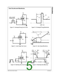
Test Circuits and Waveforms
V
BV
DSS
DS
t
P
V
DS
L
I
AS
V
DD
VARY t TO OBTAIN
P
+
-
R
REQUIRED PEAK I
G
AS
V
DD
V
GS
DUT
t
P
I
0V
AS
0
0.01Ω
t
AV
Figure 11. Unclamped Energy Test Circuit
Figure 12. Unclamped Energy Waveforms
V
DS
Q
g(TOT)
R
L
V
DS
V
= 10V
GS
V
GS
+
-
V
DD
V
GS
V
= 1V
DUT
GS
0
I
g(REF)
Q
g(TH)
Q
Q
gd
gs
I
g(REF)
0
Figure 13. Gate Charge Test Circuit
Figure 14. Gate Charge Waveforms
V
t
t
DS
ON
OFF
t
d(OFF)
t
d(ON)
t
t
f
R
L
r
V
DS
90%
90%
+
-
V
GS
V
DD
10%
10%
0
DUT
90%
50%
R
GS
V
GS
50%
PULSE WIDTH
10%
V
GS
0
Figure 15. Switching Time Test Circuit
Figure 16. Switching Time Waveform
©2002 Fairchild Semiconductor Corporation
FDH34N40 Rev. A

 FAIRCHILD [ FAIRCHILD SEMICONDUCTOR ]