Package Marking and Ordering Information
Device Marking
Device
Package
Reel Size
Tape Width
Quantity
FDH34N40
FDH34N40
TO-247
Tube
-
30
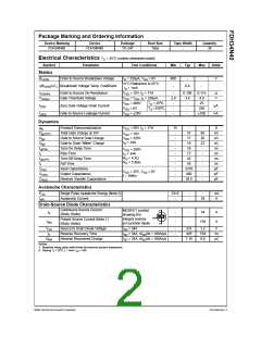
Electrical Characteristics T = 25°C (unless otherwise noted)
C
Symbol
Parameter
Test Conditions
Min
Typ
Max
Units
Statics
B
Drain to Source Breakdown Voltage
I
= 250µA, V = 0V
400
-
-
-
-
V
VDSS
D
GS
V/°C Reference to 25°C
= 1mA
∆B
/∆T Breakdown Voltage Temp. Coefficient
0.4
VDSS
J
I
D
r
Drain to Source On-Resistance
Gate Threshold Voltage
V
V
V
V
V
= 10V, I = 17A
-
0.106
0.115
4.0
Ω
DS(ON)
GS
DS
DS
GS
GS
D
V
= V , I = 250µA
2.0
3.4
V
GS(th)
GS
D
o
= 400V
T
T
= 25 C
-
-
-
-
-
-
25
C
C
I
I
Zero Gate Voltage Drain Current
Gate to Source Leakage Current
µA
nA
DSS
o
= 0V
=150 C
250
±100
= ±20V
GSS
Dynamics
g
Forward Transconductance
Total Gate Charge at 10V
Gate to Source Gate Charge
Gate to Drain “Miller” Charge
Turn-On Delay Time
Rise Time
V
= 50V, I = 17A
15
-
-
57
-
68
20
22
-
S
fs
DS
D
Q
Q
Q
nC
nC
nC
ns
ns
ns
ns
pF
pF
pF
g(TOT)
V
V
= 10V
= 320V
= 34A
GS
-
17
gs
DS
I
D
-
18
gd
t
t
t
t
-
16
d(ON)
V
I
= 200V
= 34A
= 4.3Ω
= 5.88Ω
DD
-
72
-
r
D
R
R
Turn-Off Delay Time
Fall Time
-
42
-
G
D
d(OFF)
f
-
58
-
C
C
C
Input Capacitance
-
3370
460
29.5
-
ISS
V
= 25V, V = 0V
GS
DS
Output Capacitance
Reverse Transfer Capacitance
-
-
OSS
RSS
f = 1MHz
-
-
Avalanche Characteristics
E
Single Pulse Avalanche Energy (Note 2)
Avalanche Current
2312
-
-
-
-
mJ
A
AS
I
34
AR
Drain-Source Diode Characteristics
Continuous Source Current
(Body Diode)
D
S
MOSFET symbol
showing the
integral reverse
p-n junction diode.
I
-
-
-
-
34
A
A
S
G
Pulsed Source Current (Note 1)
(Body Diode)
I
136
SM
V
Source to Drain Diode Voltage
Reverse Recovery Time
I
I
I
= 34A
-
-
-
0.9
445
7.16
1.2
534
8.6
V
SD
SD
SD
SD
t
= 34A, dI /dt = 100A/µs
ns
µC
rr
SD
Q
Reverse Recovered Charge
= 34A, dI /dt = 100A/µs
SD
RR
Notes:
1: Repetitive rating; pulse width limited by maximum junction temperature
2: Starting T = 25°C, L = 4mH, I = 34A
J
AS
©2002 Fairchild Semiconductor Corporation
FDH34N40 Rev. A

 FAIRCHILD [ FAIRCHILD SEMICONDUCTOR ]