Functional Description
UVLO: The under-voltage lockout (UVLO) circuit
guarantees the stable operation of the IC’s control circuit
by stopping and starting it as a function of the VIN value.
The UVLO circuit turns on the control circuit when VIN
exceeds 5.2V. When VIN is lower than 4.75V, the IC
start-up current is less than 100µA.
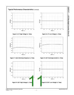
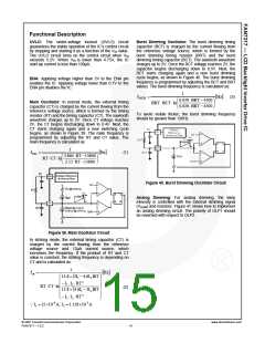
Burst Dimming Oscillator: The burst dimming timing
capacitor (BCT) is charged by the current flowing from
the reference voltage source, which is formed by the
burst dimming timing resistor (BRT) and the burst
dimming timing capacitor (BCT). The sawtooth waveform
charges up to 2V. Once the BCT voltage reaches 2V, the
capacitor begins discharging down to 0.5V. Next, the
BCT starts charging again and a new burst dimming
cycle begins, as shown in Figure 40. The burst dimming
frequency is programmed by adjusting the BCT and BRT
values. The burst dimming frequency is calculated as:
ENA: Applying voltage higher than 2V to the ENA pin
enables the IC. Applying voltage lower than 0.7V to the
ENA pin disables the IC.
1
fOSCB
=
[Hz
]
(3)
0.039⋅ BRT − 4500
0.026⋅ BRT − 4500
⎛
⎜
⎞
⎟
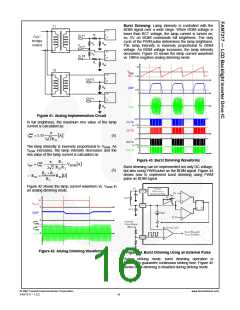
Main Oscillator: In normal mode, the external timing
capacitor (CT) is charged by the current flowing from the
reference voltage source, which is formed by the timing
resistor (RT) and the timing capacitor (CT). The sawtooth
waveform charges up to 2V. Once CT voltage reaches
2V, the CT begins discharging down to 0.4V. Next, the
CT starts charging again and a new switching cycle
begins, as shown in Figure 39. The main frequency is
programmed by adjusting the RT and CT value. The
main frequency is calculated as:
BRT ⋅ BCT ⋅ln
⎝
⎠
To avoid visible flicker, the burst dimming frequency
should be greater than 120Hz.
1
fOSC
=
[Hz
]
(1)
3.864⋅RT −13800
2.52⋅RT −13800
⎛
⎜
⎞
⎟
RT ⋅CT ⋅ln
⎝
⎠
Figure 40. Burst Dimming Oscillator Circuit
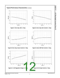
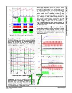
Analog Dimming: For analog dimming, the lamp
intensity is controlled with the external dimming signal
(VADIM) and resistors. Figure 41 shows how to implement
an analog dimming circuit. The polarity of OLP1 should
be reversed with respect to OLP2.
Figure 39. Main Oscillator Circuit
In striking mode, the external timing capacitor (CT) is
charged by the current flowing from the reference
voltage source and 12μA current source, which
increases the frequency. If the product of RT and CT
value is constant, the striking frequency is depending on
CT and is calculated as:
1
fstr
=
[Hz
]
⎛
⎜
⎞
⎟
13.8+
(
3I1 − 4.6I2
)
RT
2
⎜
⎜
⎜
⎟
⎟
⎟
− I1 ⋅I2 ⋅RT
13.8+
RT⋅CT⋅ln
(2)
(4.6I1 −3I2 RT
)
2
⎜
⎟
⎠
− I1 ⋅I2 ⋅RT
QI1 =12×10-6 A, I2 =1.128×10⁻³ A
⎝
© 2007 Fairchild Semiconductor Corporation
FAN7317 • 1.0.2
www.fairchildsemi.com
15

 FAIRCHILD [ FAIRCHILD SEMICONDUCTOR ]