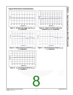
Functional Description
Startup Current
Gate Output / Soft Driving
For startup, the HV pin is connected to the line input or
bulk capacitor through an external diode and resistor,
The BiCMOS output stage is a fast totem-pole gate
driver. Cross conduction has been avoided to minimize
heat dissipation, increase efficiency, and enhance
reliability. The output driver is clamped by an internal
18V Zener diode to protect power MOSFET transistors
against undesirable gate over voltage. A soft driving
waveform is implemented to minimize EMI.
RHV, (1N4007 / 100KΩ recommended). Typical startup
current drawn from the HV pin is 3.5mA and charges
the hold-up capacitor through the diode and resistor.
When the VDD capacitor level reaches VDD-ON, the
startup current switches off. At this moment, the VDD
capacitor only supplies the FAN6753 before the
auxiliary winding of the main transformer provides the
operating current. For higher than 6KV surge test, RHV
of 100KΩ or above is recommended.
Soft-Start
For many applications, it is necessary to minimize the
inrush current at startup. The built-in 5ms soft-start
circuit significantly reduces the startup current spike
and output voltage overshoot.
Operating Current
Operating current is around 2.7mA. The low operating
current enables better efficiency and reduces the
requirement of VDD hold-up capacitance.
Built-in Slope Compensation
The sensed voltage across the current-sense resistor is
used for peak-current-mode control and pulse-by-pulse
current limiting. Built-in slope compensation improves
stability and prevents sub-harmonic oscillation.
FAN6753 inserts a synchronized, positive-going ramp at
every switching cycle.
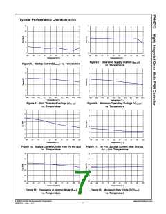
Green-Mode Operation
The proprietary green-mode function provides off-time
modulation to reduce the switching frequency in light-
load and no-load conditions. The on time is limited for
better abnormal or brownout protection. VFB, which is
derived from the voltage feedback loop, is taken as the
reference. Once VFB is lower than the threshold voltage,
the switching frequency is continuously decreased to
the minimum green-mode frequency of around 22KHz.
Constant Output Power Limit
When the SENSE voltage across sense resistor RS
reaches the threshold voltage, around 0.9V, the output
GATE drive is turned off after a small delay, tPD. This
delay introduces an additional current proportional to
tPD • VIN / LP. Since the delay is nearly constant
regardless of the input voltage VIN, higher input voltage
results in a larger additional current and the output
power limit is higher than under low input line voltage.
To compensate this variation for a wide AC input range,
a sawtooth power-limiter is designed to solve the
unequal power-limit problem. The power limiter is
designed as a positive ramp signal fed to the inverting
input of the OCP comparator. This results in a lower
current limit at high-line inputs than at low-line inputs.
Current Sensing / PWM Current Limiting
Peak-current-mode control is utilized to regulate output
voltage and provide pulse-by-pulse current limiting. The
switch current is detected by a sense resistor into the
SENSE pin. The PWM duty cycle is determined by this
current-sense signal and VFB, the feedback voltage.
When the voltage on the SENSE pin reaches around
VCOMP=(VFB–0.6)/4, the switch cycle is terminated
immediately. VCOMP is internally clamped to a variable
voltage around 0.9V for output power limit.
VDD Over-Voltage Protection (OVP)
Leading-Edge Blanking (LEB)
VDD over-voltage protection is built in to prevent
damage due to abnormal conditions. If the VDD voltage
is over the over-voltage protection voltage (VDD-OVP) and
lasts for tD-VDDOVP, the PWM pulses are disabled until
the VDD voltage drops below the UVLO, then starts
again. Over-voltage conditions are usually caused by
open feedback loops.
Each time the power MOSFET is switched on, a turn-on
spike occurs on the sense resistor. To avoid premature
termination of the switching pulse, a leading-edge
blanking time is built in. During this blanking period, the
current-limit comparator is disabled and cannot switch
off the gate driver.
Under-Voltage Lockout (UVLO)
External Latch Function (LATCH Pin)
The turn-on and turn-off thresholds are fixed internally
at 15.5V and 9.5V, respectively. During startup, the
hold-up capacitor must be charged to 15.5V through the
startup resistor to enable the IC. The hold-up capacitor
continues to supply VDD before the energy can be
delivered from auxiliary winding of the main transformer.
VDD must not drop below 9.5V during startup. This
UVLO hysteresis window ensures that the hold-up
capacitor is adequate to supply VDD during startup.
The LATCH pin can be used to control the FAN6753
entering latch mode by pulling this pin over 5.2V for
100µs. If floating, the LATCH pin is internally pulled
HIGH to 3.5V. It is not recommended to float or short
the LATCH pin to GND. This pin also includes a test
mode to disable the jitter function. LATCH pin internally
sources 100µA, so place a resistor in series to GND. Do
not let this voltage exceed 5.2V for the FAN6753 to
function normally.
© 2009 Fairchild Semiconductor Corporation
FAN6753 • Rev. 1.0.1
www.fairchildsemi.com
9

 FAIRCHILD [ FAIRCHILD SEMICONDUCTOR ]