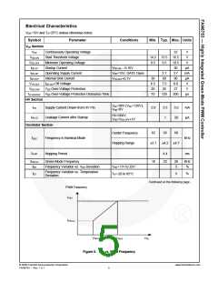
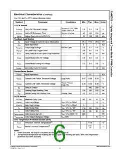
Electrical Characteristics (Continued)
VDD=15V and TA=25°C unless otherwise noted.
Symbol
Parameter
Conditions
Min. Typ. Max. Units
LATCH Section
VLATCHth > 5.2V, after
100µs Latch Off
VLATCHth
Latch-Off Threshold Voltage
5.0
5.3
5.6
V
Latch-Off De-bounce Time
tD-LATCH
ILATCH
VLATCH< VLATCHth
40
92
100
100
160
108
µs
Output Current from LATCH Pin
µA
Feedback Input Section
AV
ZFB
Input Voltage to Current-Sense Attenuation
1/4.5 1/4.0 1/3.5
V/V
kΩ
V
Input Impedance
4
7
VFB-OPEN
VFB-OLP
tD-OLP
Output High Voltage
FB Pin Open
5.0
4.6
50
5.3
4.8
56
5.6
5.0
62
FB Open-Loop Trigger Level
Delay Time of FB Pin Open-Loop Protection
V
ms
VFB-N
Green-Mode Entry FB Voltage
2.8
2.2
3.0
2.4
3.2
V
VFB-G
Green-Mode Ending FB Voltage
Zero Duty-Cycle FB Current
2.6
1.5
V
IFB-ZDC
mA
Current-Sense Section
ZSENSE Input Impedance
12
KΩ
VSTHFL
Current Limit Flatten Threshold Voltage
Current Limit Valley Threshold Voltage
0.87
0.30
0.90
0.93
0.38
Duty>40%
V
VSTHFL–VSTHVA
Duty=0%
VSTHVA
0.34
V
tPD
tLEB
TSS
Delay to Output
100
140
5.0
200
180
5.7
ns
ns
Leading-Edge Blanking Time
Period During Soft-Startup Time
100
4.3
Startup Time
ms
GATE Section
DCYMAX
VGATE-L
VGATE-H
tr
Maximum Duty Cycle
60
65
70
%
V
VDD=15V, IO=50mA
VDD=12V, IO=50mA
VDD=15V, CL=1nF
VDD=15V, CL=1nF
VDD=15V, GATE=6V
VDD=22V
Gate Low Voltage
Gate High Voltage
Gate Rising Time
Gate Falling Time
1.5
8
V
ns
ns
mA
V
150
30
250
50
350
90
tf
IGATE-SOURCE
Gate Source Current
250
VGATE-CLAMP
Gate Output Clamping Voltage
18
Over-Temperature Protection Section (OTP)
TOTP
Protection Junction Temperature(3)
+135
°C
°C
TOTP
-
TRestart
Restart Junction Temperature(4)
25
Notes:
3. When activated, the output is disabled and the latch is turned off.
4. The threshold temperature for enabling the output again and resetting the latch, after over-temperature
protection has been activated.
© 2009 Fairchild Semiconductor Corporation
FAN6753 • Rev. 1.0.1
www.fairchildsemi.com
6

 FAIRCHILD [ FAIRCHILD SEMICONDUCTOR ]