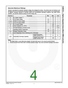
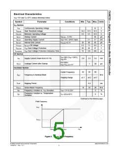
Absolute Maximum Ratings
Stresses exceeding the absolute maximum ratings may damage the device. The device may not function or be
operable above the recommended operating conditions and stressing the parts to these levels is not recommended.
In addition, extended exposure to stresses above the recommended operating conditions may affect device
reliability. The absolute maximum ratings are stress ratings only.
Symbol
VDD
Parameter
Min.
Max.
30
Unit
V
DC Supply Voltage(1, 2)
FB Pin Input Voltage
VFB
-0.3
-0.3
-0.3
7.0
V
VSENSE
VLATCH
VHV
SENSE Pin Input Voltage
LATCH Pin Input Voltage
HV Pin Input Voltage
7.0
V
7.0
V
500
400
V
Power Dissipation (TA<50°C)
PD
mW
θ JA
TJ
Thermal Resistance (Junction-to-Air)
Operating Junction Temperature
141
°C/W
°C
-40
-55
+125
+150
+260
TSTG
TL
Storage Temperature Range
°C
Lead Temperature (Wave Soldering or IR, 10 Seconds)
°C
Human Body Model,
JEDEC:JESD22-A114
5.5
kV
V
ESD
Electrostatic Discharge Capability
Charged Device Model,
JEDEC:JESD22-C101
1500
Notes:
1. All voltage values, except differential voltages, are given with respect to the network ground terminal.
2. Stresses beyond those listed under “absolute maximum ratings” may cause permanent damage to the device
© 2009 Fairchild Semiconductor Corporation
FAN6753 • Rev. 1.0.1
www.fairchildsemi.com
4

 FAIRCHILD [ FAIRCHILD SEMICONDUCTOR ]