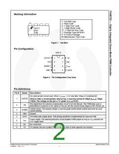
Marking Information
F: Fairchild Logo
Z: Plant Code
X: 1-Digit Year Code
Y: 1-Digit Week Code
TT: 2-Digit Die Run Code
T: Package Type (M:SOP)
P: Y=Green Package
M: Manufacture Flow Code
ZXYTT
6753
TPM
Figure 1. Top Mark
Pin Configuration
SOP-8
LATCH
FB
1
2
3
4
8
7
6
5
HV
NC
SENSE
GND
VDD
GATE
Figure 2. Pin Configuration (Top View)
Pin Definitions
Pin #
Name Description
For external latch circuit used. When VLATCHth > 5.2V and after 100µs, IC is latched off.
1
LATCH
10KΩ to GND is recommended. Internal has a sourcing current of 100µA (ILATCH), 100µA
×10KΩ. The voltage on this pin is 1V (under VLATCHth=5.2V).
The signal from the external compensation circuit is fed into this pin. The PWM duty cycle is
determined in response to the signal on this pin and the current-sense signal on the SENSE pin.
2
3
FB
Current sense. The sensed voltage is used for peak-current-mode control and cycle-by-cycle
current limiting.
SENSE
4
5
GND
Ground.
GATE
The totem-pole output driver. Soft-driving waveform is implemented for improved EMI.
Power supply. The internal protection circuit disables PWM output as long as VDD exceeds the
OVP trigger point.
6
VDD
7
8
NC
HV
No connection.
For startup, this pin is pulled HIGH to the line input or bulk capacitor via resistors.
© 2009 Fairchild Semiconductor Corporation
FAN6753 • Rev. 1.0.1
www.fairchildsemi.com
2

 FAIRCHILD [ FAIRCHILD SEMICONDUCTOR ]