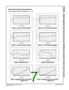
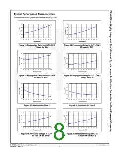
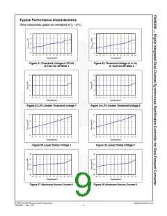
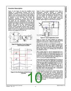
Function Description
Figure 29 and Figure 30 show the simplified circuit
diagram of a dual-forward converter and its key
waveforms. Switches Q1 and Q2 are turned on and off
together. Once Q1 and Q2 are turned on, input voltage is
applied across the transformer primary side and power
is delivered to the secondary side through the
transformer, powering D1. During this time, the
magnetizing current linearly increases. When Q1 and Q2
are turned off, the magnetizing current of the
transformer forces the reset diodes (DR1 and DR2) and
negative input voltage is applied across the transformer
primary side. During this time, magnetizing current
linearly decreases to zero and the secondary-side
inductor current freewheels through diode D2. When
synchronous rectifier SR1 and SR2 are used instead of
diodes D1 and D2, it is important to have proper timing
between drive signals for SR1 and SR2.
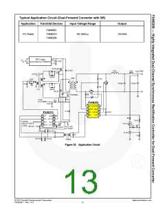
Figure 31 shows a typical application circuit. When a
dual-forward converter operates in continuous
conduction mode, the SR gate signals (GATE1 and
GATE2) are mainly controlled by SP and SN signals. SP
and SN signals are transferred through
a pulse
transformer from XP and XN signals, which are
generated by FAN6210 (Primary-Side Synchronous
Rectifier Signal Trigger for Dual Forward Converter).
Figure 31.Typical Application Circuit
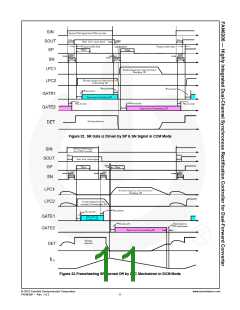
Figure 32 shows the timing diagram for continuous
conduction mode (CCM). Figure 33 shows the timing
diagram for discontinuous conduction mode (DCM).
The switching operation of SR MOSFETs Q3 and Q4 is
determined by the SN and SP signals. FAN6206 turns
on SR MOSFETs at the rising edge of the SP signal,
while it turns off the SR MOSFETs at the rising edge of
the SN signal. Within one switching cycle, SP and SN
are obtained two times.
Figure 29.Simplified Circuit Diagram of
Dual-Forward Converter
With a voltage divider R1 and R2 connected from LPC1
to secondary winding, R3 and R4 connected from LPC2
to secondary winding, the PWM timing sequences and
frequency can be tracked precisely. The SR MOSFET is
turned on by SP signal only when the voltage level on
LPC1 or LPC2 pin is pulled LOW to GND.
During PWM-on period, the rectifying SR Q3 is turned on
by the rising edge of the SP signal after a propagation
delay (tPD-HIGH-SP1) and Q3 is turned off by the rising edge
of the SN signal after a propagation delay (tPD-LOW-SN1).
During PWM-off period, the freewheeling SR Q4 is
turned on by the rising edge of the SP signal after a
propagation delay (tPD-HIGH-SP2) and Q4 is turned off by
the rising edge of the SN signal after a propagation
delay (tPD-LOW-SN2) in CCM operation.
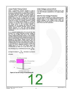
In DCM operation, the proprietary Linear-Predict Timing
Control (LPC) technique can provide synchronous
rectification control mechanism for freewheeling SR
MOSFET. Since SN signal is sent following with PWM
signal, the freewheeling SR MOSFET cannot be turned
off in time by SN signal before ILo linearly decreases to
zero. Therefore, the LPC mechanism is applied to turn
off Q3 in DCM mode.
Figure 30.Key Waveforms of Dual-Forward
Converter
© 2010 Fairchild Semiconductor Corporation
FAN6206 • Rev. 1.0.2
www.fairchildsemi.com
10

 FAIRCHILD [ FAIRCHILD SEMICONDUCTOR ]