Linear-Predict Timing Control
Under-Voltage Lockout (UVLO)
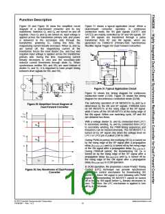
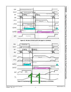
When a dual-forward converter operates in CCM or
DCM; in PWM tON period, the VIN voltage is applied to
the primary winding and the secondary inductor starts to
rise linearly and store energy. The across voltage on
secondary winding is coupled from primary winding and
proportional to VIN. The SR controller can detect this
winding voltage through a voltage divider and acquire
the VIN level. According to this detected VIN level during
PWM turn-on period, SR controller produces a charge
current ICHG to charge internal capacitor, CT, of the SR
controller. On the other hand, at PWM turn-off period,
the energy stored in the secondary inductor is
discharged. The SR controller also detects the output
voltage level to modulate discharge current IDISCHG of
internal capacitor, CT. Once the internal capacitor
voltage reaches zero, SR controller turns off SR MOS
immediately.
The power-on and off thresholds are fixed at 8.5V and
7.5V. The VDD pin is connected to a 12V output voltage
terminal.
VDD Pin Over-Voltage Protection
The over-voltage conditions are usually caused by open
feedback loops. VDD over-voltage protection is built in to
prevent damage if over voltage occurs. When the
voltage on the VDD pin exceeds 21V, the SR controller
turns off all of SR MOS operations.
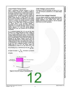
R4 is connected between the LPC2 pin and the drain
terminal of Q4. During PWM turn-on period, voltage on
the LPC2 pin is pulled HIGH due to the secondary
winding coupled from primary winding. At this moment,
SR MOS is turned off and the internal body diode of SR
MOS is reverse-biased. During PWM turn-off period, the
potential on the primary winding reverses and the
internal body diode starts to conduct output current. The
voltage on the LPC2 pin is also pulled LOW to GND. R2
is recommended as 10kΩ and the divided voltage level
on the LPC1 pin is suggested between 3V~5V. If the
voltage level of VO is 12V, the resistor values are
recommended as 105kΩ for R3 and 10kΩ for R4. The
R4
turn-off timing of Q4 is determined by the ratio
R3 + R4
R4
as Figure 34 shows. If
off earlier.
decreases, Q4 is turned
R3 + R4
Figure 34.Turn-Off Timing of Freewheeling SR
© 2010 Fairchild Semiconductor Corporation
FAN6206 • Rev. 1.0.2
www.fairchildsemi.com
12

 FAIRCHILD [ FAIRCHILD SEMICONDUCTOR ]