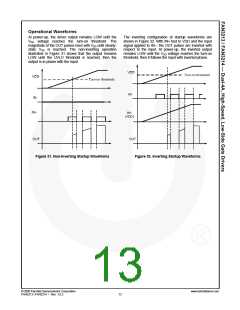
Thermal Guidelines
Gate drivers used to switch MOSFETs and IGBTs at
high frequencies can dissipate significant amounts of
power. It is important to determine the driver power
dissipation and the resulting junction temperature in the
application to ensure that the part is operating within
acceptable temperature limits.
To give a numerical example, if the synchronous rectifier
switches in the forward converter of Figure 33 are
FDMS8660S, the datasheet gives a total gate charge of
60nC at VGS = 7V, so two devices in parallel would have
120nC gate charge. At a switching frequency of 300kHz,
the total power dissipation is:
The total power dissipation in a gate driver is the sum of
P
GATE = 120nC • 7V • 300kHz • 2 = 0.504W
(5)
(6)
(7)
two components, PGATE and PDYNAMIC
:
PDYNAMIC = 7.5mA • 7V • 2 = 0.011W
PTOTAL = PGATE + PDYNAMIC
(1)
PTOTAL = 0.515W ≈ 0.52W
Gate Driving Loss: The most significant power loss
results from supplying gate current (charge per unit
time) to switch the load MOSFET on and off at the
switching frequency. The power dissipation that
results from driving a MOSFET at a specified gate-
The SOIC-8 has
a
junction-to-board thermal
characterization parameter of JB = 42°C/W. In a system
application, the localized temperature around the device
is a function of the layout and construction of the PCB
along with airflow across the surfaces. To ensure
reliable operation, the maximum junction temperature of
the device must be prevented from exceeding the
maximum rating of 150°C; with 80% derating, TJ would
be limited to 120°C. Rearranging Equation 4 determines
the board temperature required to maintain the junction
temperature below 120°C:
source voltage, VGS
, with gate charge, QG, at
switching frequency, fSW, is determined by:
PGATE = QG • VGS • fSW • n
(2)
where n is the number of driver channels in use (1 or 2).
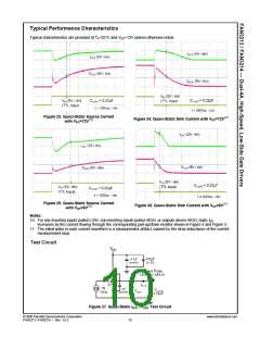
Dynamic Pre-Drive / Shoot-through Current: A power
loss resulting from internal current consumption under
dynamic operating conditions, including pin pull-up /
pull-down resistors, can be obtained using the graphs
in Typical Performance Characteristics to determine
the current IDYNAMIC drawn from VDD under actual
operating conditions:
T
B,MAX = TJ - PTOTAL
•
(8)
(9)
JB
TB,MAX = 120°C – 0.52W • 42°C/W = 98°C
PDYNAMIC = IDYNAMIC • VDD • n
(3)
Once the power dissipated in the driver is determined,
the driver junction rise with respect to circuit board can
be evaluated using the following thermal equation,
JB
assuming
was determined for a similar thermal
design (heat sinking and air flow):
TJ
= PTOTAL
•
JB + TB
(4)
where:
TJ
= driver junction temperature;
JB
= (psi) thermal characterization parameter
relating temperature rise to total power
dissipation; and
TB
= board temperature in location as defined in
the Thermal Characteristics table.
© 2008 Fairchild Semiconductor Corporation
FAN3213 / FAN3214 • Rev. 1.0.2
www.fairchildsemi.com
14

 FAIRCHILD [ FAIRCHILD SEMICONDUCTOR ]