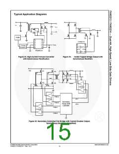
Applications Information
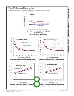
Input Thresholds
The FAN3213 and the FAN3214 drivers consist of two
identical channels that may be used independently at
rated current or connected in parallel to double the
individual current capacity.
The input thresholds meet industry-standard TTL-logic
thresholds independent of the VDD voltage, and there is
a hysteresis voltage of approximately 0.4V. These levels
permit the inputs to be driven from a range of input logic
signal levels for which a voltage over 2V is considered
logic HIGH. The driving signal for the TTL inputs should
have fast rising and falling edges with a slew rate of
6V/µs or faster, so a rise time from 0 to 3.3V should be
550ns or less. With reduced slew rate, circuit noise
could cause the driver input voltage to exceed the
hysteresis voltage and retrigger the driver input, causing
erratic operation.
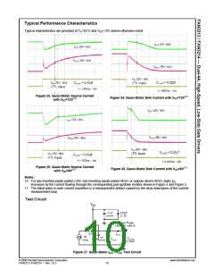
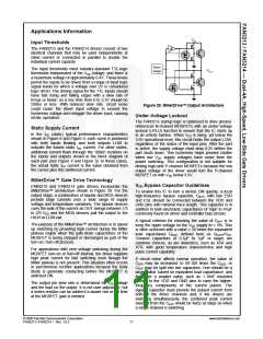
Figure 28. MillerDrive™ Output Architecture
Under-Voltage Lockout
The FAN321x startup logic is optimized to drive ground-
referenced N-channel MOSFETs with an under-voltage
lockout (UVLO) function to ensure that the IC starts up
in an orderly fashion. When VDD is rising, yet below the
3.9V operational level, this circuit holds the output LOW,
regardless of the status of the input pins. After the part
is active, the supply voltage must drop 0.2V before the
part shuts down. This hysteresis helps prevent chatter
when low VDD supply voltages have noise from the
power switching. This configuration is not suitable for
driving high-side P-channel MOSFETs because the low
output voltage of the driver would turn the P-channel
MOSFET on with VDD below 3.9V.
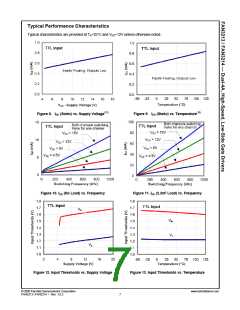
Static Supply Current
In the IDD (static) typical performance characteristics
shown in Figure 8 and Figure 9, each curve is produced
with both inputs floating and both outputs LOW to
indicate the lowest static IDD current. For other states,
additional current flows through the 100k resistors on
the inputs and outputs shown in the block diagram of
each part (see Figure 4 and Figure 5). In these cases,
the actual static IDD current is the value obtained from
the curves plus this additional current.
MillerDrive™ Gate Drive Technology
VDD Bypass Capacitor Guidelines
FAN3213 and FAN3214 gate drivers incorporate the
MillerDrive™ architecture shown in Figure 28. For the
output stage, a combination of bipolar and MOS devices
provide large currents over a wide range of supply
voltage and temperature variations. The bipolar devices
carry the bulk of the current as OUT swings between 1/3
to 2/3 VDD and the MOS devices pull the output to the
HIGH or LOW rail.
To enable this IC to turn a device ON quickly, a local
high-frequency bypass capacitor, CBYP, with low ESR
and ESL should be connected between the VDD and
GND pins with minimal trace length. This capacitor is in
addition to bulk electrolytic capacitance of 10µF to 47µF
commonly found on driver and controller bias circuits.
A typical criterion for choosing the value of CBYP is to
keep the ripple voltage on the VDD supply to ≤ 5%. This
is often achieved with a value ≥ 20 times the equivalent
The purpose of the MillerDrive™ architecture is to speed
up switching by providing high current during the Miller
plateau region when the gate-drain capacitance of the
MOSFET is being charged or discharged as part of the
turn-on / turn-off process.
load capacitance CEQV, defined here as QGATE/VDD
.
Ceramic capacitors of 0.1µF to 1µF or larger are
common choices, as are dielectrics, such as X5R and
X7R, with good temperature characteristics and high
pulse current capability.
For applications with zero voltage switching during the
MOSFET turn-on or turn-off interval, the driver supplies
high peak current for fast switching even though the
Miller plateau is not present. This situation often occurs
in synchronous rectifier applications because the body
diode is generally conducting before the MOSFET is
switched ON.
If circuit noise affects normal operation, the value of
CBYP may be increased, to 50-100 times the CEQV, or
CBYP may be split into two capacitors. One should be a
larger value, based on equivalent load capacitance, and
the other a smaller value, such as 1-10nF mounted
closest to the VDD and GND pins to carry the higher-
frequency components of the current pulses. The
bypass capacitor must provide the pulsed current from
both of the driver channels and, if the drivers are
switching simultaneously, the combined peak current
sourced from the CBYP would be twice as large as when
a single channel is switching.
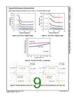
The output pin slew rate is determined by VDD voltage
and the load on the output. It is not user adjustable, but
a series resistor can be added if a slower rise or fall time
at the MOSFET gate is needed.
© 2008 Fairchild Semiconductor Corporation
FAN3213 / FAN3214 • Rev. 1.0.2
www.fairchildsemi.com
11

 FAIRCHILD [ FAIRCHILD SEMICONDUCTOR ]