Layout and Connection Guidelines
The FAN3213 and FAN3214 gate drivers incorporate
fast-reacting input circuits, short propagation delays,
and powerful output stages capable of delivering current
peaks over 4A to facilitate voltage transition times from
under 10ns to over 150ns. The following layout and
connection guidelines are strongly recommended:
.
Keep high-current output and power ground paths
separate from logic input signals and signal ground
paths. This is especially critical for TTL-level logic
thresholds at driver input pins.
.
Keep the driver as close to the load as possible to
minimize the length of high-current traces. This
reduces the series inductance to improve high-
speed switching, while reducing the loop area that
can radiate EMI to the driver inputs and surrounding
circuitry.
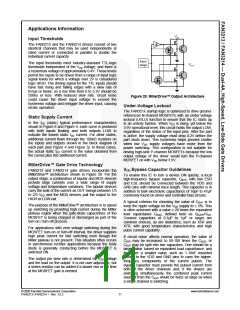
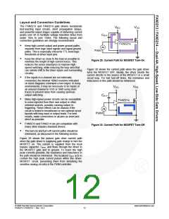
Figure 29. Current Path for MOSFET Turn-On
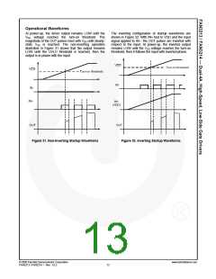
Figure 30 shows the current path when the gate driver
turns the MOSFET OFF. Ideally, the driver shunts the
current directly to the source of the MOSFET in a small
circuit loop. For fast turn-off times, the resistance and
inductance in this path should be minimized.
.
.
If the inputs to a channel are not externally
connected, the internal 100k resistors indicated
on block diagrams command a low output. In noisy
environments, it may be necessary to tie inputs of
an unused channel to VDD or GND using short
traces to prevent noise from causing spurious
output switching.
Many high-speed power circuits can be susceptible
to noise injected from their own output or other
external sources, possibly causing output re-
triggering. These effects can be obvious if the
circuit is tested in breadboard or non-optimal circuit
layouts with long input or output leads. For best
results, make connections to all pins as short and
direct as possible.
.
.
FAN3213 and FAN3214 are pin-compatible with
many other industry-standard drivers.
Figure 30. Current Path for MOSFET Turn-Off
The turn-on and turn-off current paths should be
minimized, as discussed in the following section.
Figure 29 shows the pulsed gate drive current path
when the gate driver is supplying gate charge to turn the
MOSFET on. The current is supplied from the local
bypass capacitor, CBYP, and flows through the driver to
the MOSFET gate and to ground. To reach the high
peak currents possible, the resistance and inductance in
the path should be minimized. The localized CBYP acts to
contain the high peak current pulses within this driver-
MOSFET circuit, preventing them from disturbing the
sensitive analog circuitry in the PWM controller.
© 2008 Fairchild Semiconductor Corporation
FAN3213 / FAN3214 • Rev. 1.0.2
www.fairchildsemi.com
12

 FAIRCHILD [ FAIRCHILD SEMICONDUCTOR ]