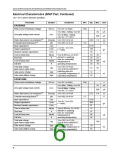
KA5S-SERIES KA5S0765C/KA5S09654QT/KA5S0965/KA5S12656/KA5S1265
Electrical Characteristics (SFET Part; Continued)
(Ta = 25°C unless otherwise specified)
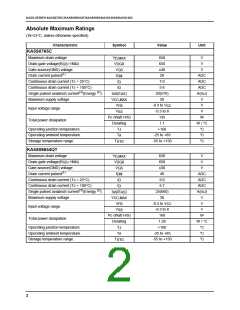
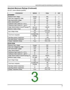
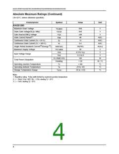
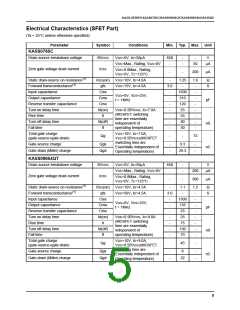
Parameter
Symbol
Conditions
Min. Typ. Max. Unit
KA5S0965
Drain-source breakdown voltage
BVDSS
IDSS
VGS=0V, ID=50µA
650
-
-
-
-
V
VDS=Max., Rating, VGS=0V
50
µA
Zero gate voltage drain current
VDS=0.8Max., Rating,
VGS=0V, TC=125°C
-
-
200
µA
Static drain-source on resistance(1)
Forward transconductance(1)
Input capacitance
RDS(on)
gfs
VGS=10V, ID=4.5A
VDS=50V, ID=4.5A
-
0.96
-
1.2
-
Ω
5.0
S
Ciss
Coss
Crss
td(on)
tr
-
-
-
-
-
-
-
1750
190
78
-
VGS=0V, VDS=25V,
f = 1MHz
Output capacitance
Reverse transfer capacitance
Turn on delay time
-
pF
nS
-
VDD=0.5BVDSS, ID=9.0A
(MOSFET switching
time are essentially
independent of
20
50
55
180
70
Rise time
23
Turn off delay time
td(off)
tf
85
Fall time
operating temperature)
30
Total gate charge
(gate-source+gate-drain)
VGS=10V, ID=9.0A,
VDS=0.5BVDSS(MOSFET
Switching time are
Essentially independent of
Operating temperature)
Qg
-
74
95
Gate-source charge
Qgs
Qgd
-
-
12
35
-
-
nC
Gate-drain (Miller) charge
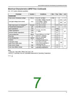
KA5S12656
Drain-source breakdown voltage
BVDSS
IDSS
VGS=0V, ID=50µA
650
-
-
-
-
V
VDS=Max., Rating, VGS=0V
50
µA
Zero gate voltage drain current
VDS=0.8Max., Rating,
VGS=0V, TC=125°C
-
-
200
µA
Static drain-source on resistance(1)
Forward transconductance(1)
Input capacitance
RDS(on)
gfs
VGS=10V, ID=6.0A
VDS=50V, ID=4.0A
-
0.72
-
0.9
Ω
5.7
-
-
-
-
-
-
-
-
S
Ciss
Coss
Crss
td(on)
tr
-
-
-
-
-
-
-
2700
300
61
VGS=0V, VDS=25V,
f = 1MHz
Output capacitance
Reverse transfer capacitance
Turn on delay time
pF
nS
VDD=0.5BVDSS, ID=12.0A
(MOSFET switching
time are essentially
independent of
18
Rise time
37
Turn off delay time
td(off)
tf
88
Fall time
operating temperature)
36
Total gate charge
(gate-source+gate-drain)
VGS=10V, ID=12.0A,
VDS=0.5BVDSS(MOSFET
Switching time are
Essentially independent of
Operating temperature)
Qg
-
-
140
Gate-source charge
Qgs
Qgd
-
-
20
69
-
-
nC
Gate-drain (Miller) charge
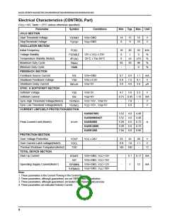
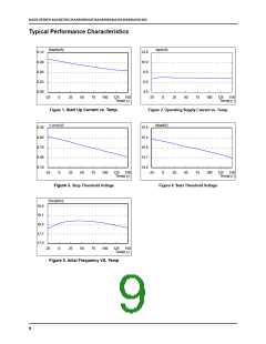
6

 FAIRCHILD [ FAIRCHILD SEMICONDUCTOR ]