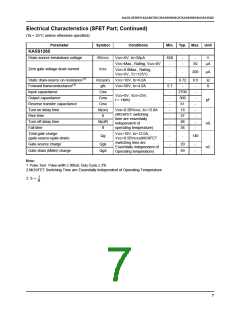
KA5S-SERIES KA5S0765C/KA5S09654QT/KA5S0965/KA5S12656/
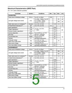
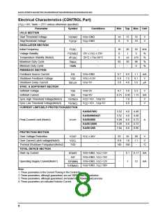
Electrical Characteristics (SFET Part)
(Ta = 25°C unless otherwise specified)
Parameter
Symbol
Conditions
Min. Typ. Max. Unit
KA5S0765C
Drain-source breakdown voltage
BVDSS
IDSS
VGS=0V, ID=50µA
650
-
-
-
-
V
VDS=Max., Rating, VGS=0V
50
µA
Zero gate voltage drain current
VDS=0.8Max., Rating,
VGS=0V, TC=125°C
-
-
200
µA
Static drain-source on resistance(1)
Forward transconductance(1)
Input capacitance
RDS(on)
gfs
VGS=10V, ID=4.0A
VDS=15V, ID=4.0A
-
1.25
-
1.6
Ω
3.0
-
-
-
-
-
-
-
-
S
Ciss
Coss
Crss
td(on)
tr
-
-
-
-
-
-
-
1600
310
120
25
VGS=0V, VDS=25V,
f = 1MHz
Output capacitance
Reverse transfer capacitance
Turn on delay time
pF
nS
VDD=0.5BVDSS, ID=7.0A
(MOSFET switching
time are essentially
independent of
Rise time
55
Turn off delay time
td(off)
tf
80
Fall time
operating temperature)
50
Total gate charge
(gate-source+gate-drain)
VGS=10V, ID=7.0A,
VDS=0.5BVDSS(MOSFET
Switching time are
Essentially independent of
Operating temperature)
Qg
-
-
72
Gate-source charge
Qgs
Qgd
-
-
9.3
-
-
nC
Gate-drain (Miller) charge
29.3
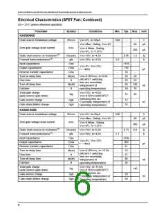
KA5S09654QT
Drain-source breakdown voltage
BVDSS
IDSS
VGS=0V, ID=50µA
650
-
-
-
-
V
VDS=Max., Rating, VGS=0V
200
µA
Zero gate voltage drain current
VDS=0.8Max., Rating,
VGS=0V, TC=125°C
-
-
300
µA
Static drain-source on resistance(1)
Forward transconductance(1)
Input capacitance
RDS(on)
gfs
VGS=10V, ID=4.5A
VDS=50V, ID=4.5A
-
1.1
-
1.2
Ω
3.0
-
-
-
-
-
-
-
-
S
Ciss
Coss
Crss
td(on)
tr
-
-
-
-
-
-
-
1300
135
25
VGS=0V, VDS=25V,
f = 1MHz
Output capacitance
Reverse transfer capacitance
Turn on delay time
pF
nS
VDD=0.5BVDSS, ID=9.0A
(MOSFET switching
time are essentially
independent of
25
Rise time
75
Turn off delay time
td(off)
tf
130
70
Fall time
operating temperature)
Total gate charge
(gate-source+gate-drain)
VGS=10V, ID=9.0A,
VDS=0.5BVDSS(MOSFET
Switching time are
Essentially independent of
Operating temperature)
Qg
45
-
Gate-source charge
Qgs
Qgd
-
-
8
-
-
nC
Gate-drain (Miller) charge
22
5

 FAIRCHILD [ FAIRCHILD SEMICONDUCTOR ]