xr
XR16L2552
2.25V TO 5.5V DUART WITH 16-BYTE FIFO
REV. 1.1.1
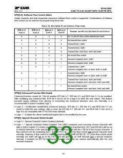
MCR[0]: DTR# Output
The DTR# pin is a modem control output. If the modem interface is not used, this output may be used as a
general purpose output.
• Logic 0 = Force DTR# output to a logic 1 (default).
• Logic 1 = Force DTR# output to a logic 0.
MCR[1]: RTS# Output
The RTS# pin is a modem control output. If the modem interface is not used, this output may be used as a
general purpose output.
• Logic 0 = Force RTS# output to a logic 1 (default).
• Logic 1 = Force RTS# output to a logic 0.
MCR[2]: OP1# Output
OP1# is not available as an output pin on the L2552. But it is available for use during Internal Loopback Mode.
In the Loopback Mode, this bit is used to write the state of the modem RI# interface signal.
MCR[3]: OP2# Output
OP2# is available as an output pin on the L2552 when AFR[2:1] = ‘00’. In the Loopback Mode, MCR[3] is used
to write the state of the modem CD# interface signal. Also see pin descriptions for MF# pins.
• Logic 0 = Forces OP2# output to a logic 1 (default).
• Logic 1 = Forces OP2# output to a logic 0.
MCR[4]: Internal Loopback Enable
• Logic 0 = Disable loopback mode (default).
• Logic 1 = Enable local loopback mode, see loopback section and Figure 13.
MCR[5]: Xon-Any Enable
• Logic 0 = Disable Xon-Any function (for 16C550 compatibility, default).
• Logic 1 = Enable Xon-Any function. In this mode, any RX character received will resume transmit operation.
The RX character will be loaded into the RX FIFO , unless the RX character is an Xon or Xoff character and
the L2552 is programmed to use the Xon/Xoff flow control.
MCR[6]: Infrared Encoder/Decoder Enable
• Logic 0 = Enable the standard modem receive and transmit input/output interface. (Default)
• Logic 1 = Enable infrared IrDA receive and transmit inputs/outputs. The TX/RX output/input are routed to the
infrared encoder/decoder. The data input and output levels conform to the IrDA infrared interface
requirement. While in this mode, the infrared TX output will be a logic 0 during idle data conditions.
MCR[7]: Clock Prescaler Select
• Logic 0 = Divide by one. The input clock from the crystal or external clock is fed directly to the Programmable
Baud Rate Generator without further modification, i.e., divide by one (default).
• Logic 1 = Divide by four. The prescaler divides the input clock from the crystal or external clock by four and
feeds it to the Programmable Baud Rate Generator, hence, data rates become one forth.
4.9
Line Status Register (LSR) - Read Only
This register provides the status of data transfers between the UART and the host.
LSR[0]: Receive Data Ready Indicator
• Logic 0 = No data in receive holding register or FIFO (default).
• Logic 1 = Data has been received and is saved in the receive holding register or FIFO.
29

 EXAR [ EXAR CORPORATION ]