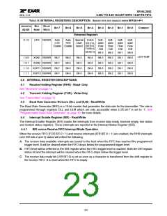
xr
XR16L2552
2.25V TO 5.5V DUART WITH 16-BYTE FIFO
REV. 1.1.1
2.19
Sleep Mode with Auto Wake-Up
The L2552 supports low voltage system designs, hence, a sleep mode is included to reduce its power
consumption when the chip is not actively used.
All of these conditions must be satisfied for the L2552 to enter sleep mode:
■ no interrupts pending for both channels of the L2552 (ISR bit-0 = 1)
■ divisor is a non-zero value (ie. DLL = 0x1)
■ sleep mode of both channels are enabled (IER bit-4 = 1)
■ modem inputs are not toggling (MSR bits 0-3 = 0)
■ RX input pins are idling at a logic 1
The L2552 stops its crystal oscillator to conserve power in the sleep mode. User can check the XTAL2 pin for
no clock output as an indication that the device has entered the sleep mode.
The L2552 resumes normal operation by any of the following:
■ a receive data start bit transition (logic 1 to 0)
■ a data byte is loaded to the transmitter, THR or FIFO
■ a change of logic state on any of the modem or general purpose serial inputs: CTS#, DSR#, CD#, RI#
If the L2552 is awakened by any one of the above conditions, it will return to the sleep mode automatically after
all interrupting conditions have been serviced and cleared. If the L2552 is awakened by the modem inputs, a
read to the MSR is required to reset the modem inputs. In any case, the sleep mode will not be entered while
an interrupt is pending from channel A or B. The L2552 will stay in the sleep mode of operation until it is
disabled by setting IER bit-4 to a logic 0.
If the address lines, data bus lines, IOW#, IOR#, CSA#, CSB#, and modem input lines remain steady when the
L2552 is in sleep mode, the maximum current will be in the microamp range as specified in the DC Electrical
Characteristics on page 36. If the input lines are floating or are toggling while the L2552 is in sleep mode, the
current can be up to 100 times more. If any of those signals are toggling or floating, then an external buffer
would be required to keep the address, data and control lines steady to achieve the low current. As an
alternative, please refer to the XR16L2551 with the PowerSave feature that eliminates any unnecessary
external buffer.
A word of caution: owing to the starting up delay of the crystal oscillator after waking up from sleep mode, the
first few receive characters may be lost. The number of characters lost during the restart also depends on your
operating data rate. More characters are lost when operating at higher data rate. Also, it is important to keep
RX A/B inputs idling at logic 1 or “marking” condition during sleep mode to avoid receiving a “break” condition
upon the restart. This may occur when the external interface transceivers (RS-232, RS-485 or another type)
are also put to sleep mode and cannot maintain the “marking” condition. To avoid this, the designer can use a
47k-100k ohm pull-up resistor on the RXA and RXB pins.
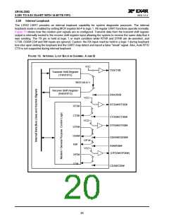
19

 EXAR [ EXAR CORPORATION ]