áç
ST16C650A
2.90V TO 5.5V UART WITH 32-BYTE FIFO
REV. 5.0.0
MSR[6]: RI Input Status
RI# (active high, logical 1). Normally this bit is the compliment of the RI# input. In the loopback mode this bit is
equivalent to bit-2 in the MCR register. The RI# input may be used as a general purpose input when the
modem interface is not used.
MSR[7]: CD Input Status
CD# (active high, logical 1). Normally this bit is the compliment of the CD# input. In the loopback mode this bit
is equivalent to bit-3 in the MCR register. The CD# input may be used as a general purpose input when the
modem interface is not used.
4.11 Infrared Transmit Pulse Width Control Register (IRPW) - Write Only
The IRPW register allows the user to program the encoder’s pulse width. This cuts the LED on-time, hence,
reducing power consumption.
IRPW [7:0]: Pulse width control
A 0x00 value (default) will set the pulse width to normal width of 3/16 of the data bit rate. The programmable
infrared pulse width can be calculated using the following equation:
• Infrared pulse width (PW) = Crystal clock period x ‘N’, where ‘N’ is the value in IRPW from 1 to 255.
Examples:
Crystal frequency = 14.7456MHz (clock period of 67.82ns)
PW = 67.82 x ‘N’ or ranges from 67.82ns to 17.29ms
Caution: Never allow PW to exceed the operating data rate bit period, else the encoder stops.
4.12 Scratch Pad Register (SPR)
This is an 8-bit general purpose register for the user to store temporary data. The content of this register is
preserved during sleep mode but becomes 0xFF (default) after a reset or a power off-on cycle.
4.13 Baud Rate Generator Divisors (DLL and DLM) - Read/Write
The Baud Rate Generator (BRG) is a 16-bit counter that generates the data rate for the transmitter. The rate is
programmed through registers DLL and DLM which are only accessible when LCR bit-7 is set to ‘1’. See
Programmable Baud Rate Generator section for more details. The concatenation of the contents of DLM and
DLL gives the 16-bit divisor value which is used to calculate the baud rate:
• Baud Rate = (Clock Frequency / 16) / Divisor
Also see MCR bit-7 and Table 4.
4.14 Device Identification Register (DVID) - Read Only
This register contains the device ID (0x04 for ST16C650A). Prior to reading this register, DLL and DLM should
be set to 0x00.
4.15 Device Revision Register (DREV) - Read Only
This register contains the device revision information. For example, 0x01 means revision A. Prior to reading
this register, DLL and DLM should be set to 0x00.
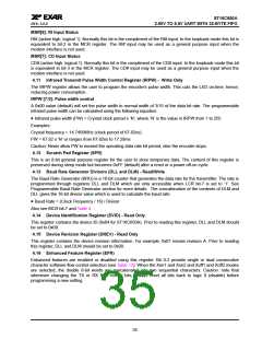
4.16 Enhanced Feature Register (EFR)
Enhanced features are enabled or disabled using this register. Bit 0-3 provide single or dual consecutive
character software flow control selection (see Table 12). When the Xon1 and Xon2 and Xoff1 and Xoff2 modes
are selected, the double 8-bit words are concatenated into two sequential characters. Caution: note that
whenever changing the TX or RX flow control bits, always reset all bits back to logic 0 (disable) before
programming a new setting.
35

 EXAR [ EXAR CORPORATION ]