Document No.: FT_000288
FT232H SINGLE CHANNEL HI-SPEED USB TO MULTIPURPOSE UART/FIFO IC
Datasheet Version 1.8
Clearance No.: FTDI #199
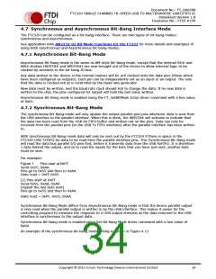
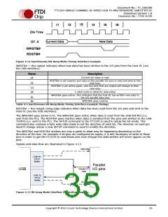
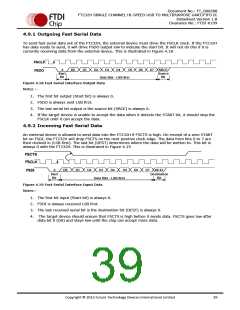
WRSTB#
RDSTB#
Figure 4.12 Synchronous Bit-Bang Mode Timing Interface Example
WRSTB# = this output indicates when new data has been written to the I/O pins from the Host PC (via
the USB interface).
Name
Description
Current pin state is read
t1
RDSTB# is set inactive and data on the parallel I/O pins is read and sent to the
t2
USB host.
RDSTB# is set active again, and any pins that are output will change to their
new data
T3
t4
1 clock cycle to allow for data setup
WRSTB# goes active. This indicates that the host PC has written new data to
the I/O parallel data pins
t5
t6
WRSTB# goes inactive
Table 4.3 Synchronous Bit-Bang Mode Timing Interface Example Timings
RDSTB# = this output rising edge indicates when data has been read from the I/O pins and sent to the
Host PC (via the USB interface).
The WRSTB# goes active in t5. The WRSTB# goes active when data is read from the USB RXFIFO (i.e.
sent from the PC). The RDSTB# goes inactive when data is sampled from the pins and written to the USB
TXFIFO (i.e. sent to the PC). The SETUP command to the FT232H is used to setup the bit-mode. This
command also contains a byte wide data mask to set the direction of each bit. The direction on each pin
doesn’t change unless a new SETUP command is used to modify the direction.
The WRSTB# and RDSTB# strobes are only a guide to what may be happening depending on the
direction of the bus. For example if all pins are configured as inputs, it is still necessary to write to these
pins in order to get the FT232H to read those pins even though the data written will never appear on the
pins.
Signals and data-flow are illustrated in Figure 4.13
WRSTB#
USB Rx
FIFO/
Buffer
Parallel
I/O pins
Parallel I/O
USB
data
USB Tx
FIFO/
Buffer
RDSTB#
Figure 4.13 Bit-bang Mode Dataflow Illustration Diagram.
Copyright © 2012 Future Technology Devices International Limited
35

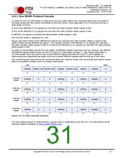
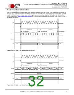
 ETC [ ETC ]