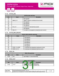
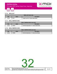
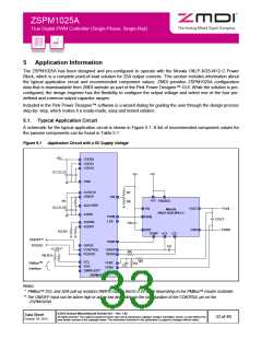
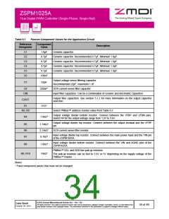
ZSPM1025A
True Digital PWM Controller (Single-Phase, Single-Rail)
5.1.1.
Output Voltage Selection
The ZSPM1025A can be configured to operate within two output voltage ranges (see Table 5.2). If the required
output voltage is within range #1 resistor R4 should not be placed on the application board. For output voltages
within range #2, resistor R4 should be placed on the application board.
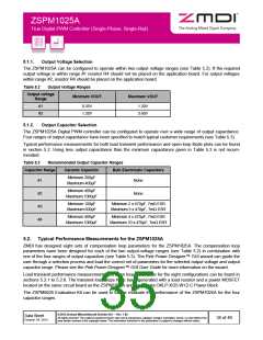
Table 5.2
Output Voltage Ranges
Output voltage
Range
Minimum VOUT
Maximum VOUT
#1
#2
0.35V
1.20V
1.20V
3.60V
5.1.2.
Output Capacitor Selection
The ZSPM1025A Digital PWM controller can be configured to operate over a wide range of output capacitance.
Four ranges of output capacitance have been specified to match typical customer requirements (see Table 5.3).
Typical performance measurements for both load transient performance and open-loop Bode plots can be found
in section 5.2. Using less output capacitance than the minimum capacitance given in Table 5.3 is not recom-
mended.
Table 5.3
Recommended Output Capacitor Ranges
Capacitor Range
Ceramic Capacitor
Bulk Electrolytic Capacitors
Minimum 200µF
Maximum 400µF
#1
None
Minimum 400µF
#2
#3
#4
None
Maximum 1000µF
Minimum 100µF
Maximum 600µF
Minimum 2 x 470µF, 7mΩ ESR
Maximum 5 x 470µF, 7mΩ ESR
Minimum 400µF
Minimum 4 x 470µF, 7mΩ ESR
Maximum 10 x 470µF, 7mΩ ESR
Maximum 1000µF
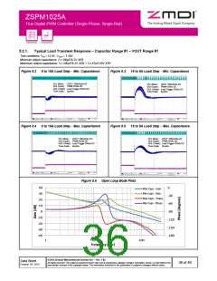
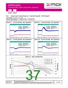
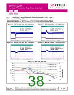
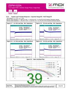
5.2. Typical Performance Measurements for the ZSPM1025A
ZMDI has designed eight sets of compensation loop parameters for the ZSPM1025A. The compensation loop
parameters have been designed for each of the two output-voltage ranges (see Table 5.2) in combination with
one of the four ranges of output capacitors (see Table 5.3). The Pink Power Designer™ GUI wizard can guide the
user through a selection process and load the correct set of parameters for the selected output voltage and output
capacitor range. Please see the Pink Power Designer™ GUI User Guide for more information on the wizard.
Load transient performance measurements and open loop Bode plots for the eight configurations can be found in
sections 5.2.1 to 5.2.8. The transient load steps have been generated with a load resistor and a power MOSFET
located on the same circuit board as the ZSPM1025A and the Murata OKLP-X/25-W12-C Power Block.
The ZSPM8025 Evaluation Kit can be used to further evaluate the performance of the ZSPM1025A for the four
capacitor ranges.
© 2013 Zentrum Mikroelektronik Dresden AG — Rev. 1.00
All rights reserved. The material contained herein may not be reproduced, adapted, merged, translated, stored, or used without the
prior written consent of the copyright owner. The information furnished in this publication is subject to changes without notice.
Data Sheet
October 24, 2013
35 of 46

 ETC [ ETC ]