Page 66
Epson Research and Development
Vancouver Design Center
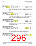
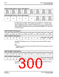
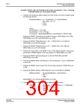
REG[10Ch] BitBLT Memory Address Offset Register 0
BitBLT
Memory
BitBLT
Memory
BitBLT
Memory
BitBLT
Memory
BitBLT
Memory
BitBLT
Memory
BitBLT
Memory
BitBLT
Memory
Address
Address
Address
Address
Address
Address
Address
Address
Offset Bit 7
Offset Bit 6
Offset Bit 5
Offset Bit 4
Offset Bit 3
Offset Bit 2
Offset Bit 1
Offset Bit 0
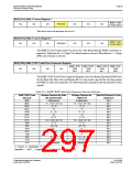
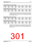
REG[10Dh] BitBLT Memory Address Offset Register 1
BitBLT
Memory
Address
BitBLT
Memory
Address
BitBLT
Memory
Address
n/a
n/a
n/a
n/a
n/a
Offset Bit 10
Offset Bit 9
Offset Bit 8
The BitBLT Memory Address Offset Registers form the BitBLTs 11-bit address offset
from the starting word of line “n” to the starting word of line “n + 1”. They are used for
address calculation only when the BitBLT is configured as a rectangular region of memory
using the BitBLT Destination/Source Linear Select bits (REG[100h] bits 1-0). They are not
used for the displays.
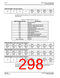
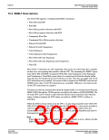
REG[110h] BitBLT Width Register 0
BitBLT Width BitBLT Width BitBLT Width BitBLT Width BitBLT Width BitBLT Width BitBLT Width BitBLT Width
Bit 7
REG[111h] BitBLT Width Register 1
n/a n/a n/a
Bit 6
Bit 5
Bit 4
Bit 3
Bit 2
Bit 1
Bit 0
BitBLT Width BitBLT Width
Bit 9 Bit 8
n/a
n/a
n/a
The BitBLT Width Registers form a 10-bit register that specifies the BitBLT width in
pixels less 1.
Note
The BitBLT operations Pattern Fill with ROP and Pattern Fill with transparency require
a BitBLT Width ≥ 2.
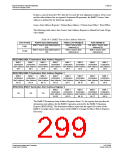
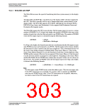
REG[112h] BitBLT Height Register 0
BitBLT Height BitBLT Height BitBLT Height BitBLT Height BitBLT Height BitBLT Height BitBLT Height BitBLT Height
Bit 7
Bit 6
Bit 5
Bit 4
Bit 3
Bit 2
Bit 1
Bit 0
REG[113h] BitBLT Height Register 1
BitBLT Height BitBLT Height
Bit 9 Bit 8
n/a
n/a
n/a
n/a
n/a
n/a
The BitBLT Height Registers form a 10-bit register that specifies the BitBLT height in
pixels less 1.
S1D13506
X25B-G-003-03
Programming Notes and Examples
Issue Date: 01/02/06

 EPSON [ EPSON COMPANY ]