Page 182
Epson Research and Development
Vancouver Design Center
10 Display Buffer
The system addresses the display buffer through the CS#, M/R#, and AB[20:0] input pins.
When CS# = 0 and M/R# = 1, the display buffer is addressed by bits AB[20:0]. See the table
below:
Table 10-1: S1D13506 Addressing
CS#
M/R#
Access
Register access - see Section 8.2, “Register Mapping” on
page 124.
• REG[000h] is addressed when AB[12:0] = 0
• REG[001h] is addressed when AB[12:0] = 1
• REG[n] is addressed when AB[12:0] = n
0
0
Memory access: the 2M byte display buffer is addressed by
AB[20:0]
0
1
1
X
S1D13506 not selected
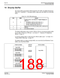
The display buffer address space is always 2M bytes. However, the physical display buffer
may be either 512K bytes or 2M bytes – see Section 5.3, “Summary of Configuration
Options” on page 39.
A 512K byte display buffer is replicated in the 2M byte address space – see Figure 10-1:
“Display Buffer Addressing,” on page 182.
The display buffer can contain an image buffer, one or more Ink Layer/Hardware Cursor
buffers, and a Dual Panel Buffer.
512K Byte Buffer
AB[20:0]
2M Byte Buffer
000000h
Image Buffer
Ink/Cursor Buffer
Dual Panel Buffer
Image Buffer
07FFFFh
080000h
Image Buffer
Ink/Cursor Buffer
Dual Panel Buffer
0FFFFFh
100000h
Image Buffer
Ink/Cursor Buffer
Dual Panel Buffer
17FFFFh
180000h
Image Buffer
Ink/Cursor Buffer
Dual Panel Buffer
Ink/Cursor Buffer
Dual Panel Buffer
1FFFFFh
Figure 10-1: Display Buffer Addressing
S1D13506
X25B-A-001-10
Hardware Functional Specification
Issue Date: 01/02/06

 EPSON [ EPSON COMPANY ]