Page 184
Epson Research and Development
Vancouver Design Center
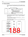
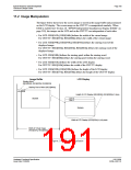
11 Display Configuration
11.1 Display Mode Data Format
The following diagrams show the display mode data formats for a little endian system:
.
4 bpp:
Byte 0
bit 7
bit 0
P P P P
P P P P
3
4
0
1
2
7
5
6
A
A
A
B
B
B
C
C
C
D
D
D
A
A
A
B
B
B
C
C
C
D
D
D
0
2
4
0
2
4
0
2
4
0
2
4
1
3
5
1
3
5
1
3
5
1
3
5
Byte 1
Byte 2
P
= (A , B , C , D )
n n n n
n
Panel Display
P P P P
P P P P
3
4
Host Address
8 bpp:
Display Buffer
bit 7
bit 0
0
1
2
5
6
7
G
F
F
F
H
0
D
D
D
Byte 0
Byte 1
Byte 2
A
0
B
C
E
E
E
0
1
2
0
0
0
0
1
2
0
1
2
G
G
B
B
C
C
H
1
A
1
1
2
1
2
1
2
P
= (A , B , C , D ,E , F , G , H )
n
n
n
n
n
n
n
n
n
H
2
A
2
Panel Display
Host Address
Display Buffer
15 bpp:
5-5-5 RGB
bit 7
2
bit 0
0
P P P P
P P P P
0
1
2
3
4
5
6
7
1
4
0
4
2
1
3
G
0
G
B
0
G
R
B
B
0
B
B
0
0
Byte 0
Byte 1
Byte 2
Byte 3
0
0
0
4-0
4-0
4-0
4
3
P
= (R
, G
, B
n
)
2
1
0
3
n
n
n
G
B
R
G
R
B
R
B
G
0
R
B
0
0
0
0
0
0
2
1
0
4
2
1
3
0
G
1
G
R
B
1
1
1
1
1
1
1
4
3
4
2
1
0
3
G
G
1
R
R
R
R
1
1
1
1
1
1
Panel Display
Host Address
16 bpp:
Display Buffer
5-6-5 RGB
P P P P
3
P P P P
0
1
2
4
5
6
7
bit 7
2
bit 0
0
1
4
3
0
1
2
G
0
G
G
B
B
0
B
0
B
B
0
0
Byte 0
Byte 1
Byte 2
Byte 3
0
0
0
4
3
1
2
4
0
5
3
4-0
5-0
4-0
R
0
R
R
0
R
G
0
R
B
G
B
G
0
P
= (R
, G
, B
n
)
0
0
0
0
n
n
n
2
1
4
0
1
3
2
0
G
1
G
R
B
1
G
R
B
1
B
1
1
1
1
1
4
3
1
2
5
4
0
3
R
1
R
1
Panel Display
R
G
G
1
G
1
1
1
1
1
Host Address
Display Buffer
Figure 11-1: 4/8/15/16 Bit-per-pixel Format Memory Organization
Note
1. The Host-to-Display mapping shown here is for a little endian system.
2. For 15/16 bit-per-pixel formats, R , G , B represent the red, green, and blue color
n
n
n
components.
S1D13506
X25B-A-001-10
Hardware Functional Specification
Issue Date: 01/02/06

 EPSON [ EPSON COMPANY ]