Epson Research and Development
Page 107
Vancouver Design Center
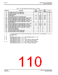
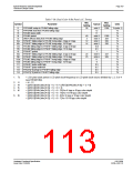
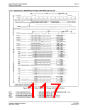
Table 7-30: Dual Color 8-Bit Panel A.C. Timing
Min.
Setting
Max.
Setting
1268
Symbol
Parameter
Typical
Units
t1
t2
FPFRAME setup to FPLINE falling edge
FPFRAME hold from FPLINE falling edge
28
note 2
12
Ts (note 1)
Ts
t3
FPLINE pulse width
11
Ts
t4
t5
FPLINE period
40
3
12
14
note 3
note 4
note 5
note 5
10.5
8.5
1280
259
236
238
Ts
Ts
Ts
Ts
Ts
Ts
Ts
DRDY (MOD) delay from FPLINE falling edge
FPSHIFT falling edge to FPLINE rising edge, 4 bpp or 8 bpp
FPSHIFT falling edge to FPLINE rising edge, 15/16 bpp
FPLINE falling edge to FPSHIFT falling edge, 4 bpp or 8 bpp
FPLINE falling edge to FPSHIFT falling edge, 15/16 bpp
FPSHIFT period
t6a
t6b
t7a
t7b
t8
1
t9a
t9b
t10a
t10b
t11
t12
t13
t14
FPSHIFT falling edge to FPLINE falling edge, 4 bpp or 8 bpp
FPSHIFT falling edge to FPLINE falling edge, 15/16 bpp
FPLINE falling edge to FPSHIFT rising edge, 4 bpp or 8 bpp
FPLINE falling edge to FPSHIFT rising edge, 15/16 bpp
FPSHIFT pulse width high
FPSHIFT pulse width low
FPDAT[7:0] setup to FPSHIFT falling edge
FPDAT[7:0] hold to FPSHIFT falling edge
23
25
note 6
note 6
11
9
0.5
0.5
0.5
0.5
247
249
Ts
Ts
Ts
Ts
Ts
Ts
Ts
Ts
1. Ts
= LCD pixel clock period. LCD pixel clock frequency is LCD pixel clock source divided by 1, 2, 3 or 4
(see REG[014h]).
2. t1
3. t4
4. t5
5. t6
= t4 - 12
= [((REG[032h] bits [6:0]) + 1) × 8 + ((REG[034h] bits [4:0]) + 1) × 8]
= [((REG[034h] bits [4:0]) + 1) × 8 + 3]
= [((REG[034h] bits [4:0]) + 1) × 8 - 20] for 4 bpp or 8 bpp color depth
= [((REG[034h] bits [4:0]) + 1) × 8 - 18] for 15/16 bpp color depth
= [((REG[034h] bits [4:0]) + 1) × 8 - 9] for 4 bpp or 8 bpp color depth
= [((REG[034h] bits [4:0]) + 1) × 8 - 7] for 15/16 bpp color depth
6. t9
Hardware Functional Specification
Issue Date: 01/02/06
S1D13506
X25B-A-001-10

 EPSON [ EPSON COMPANY ]