Preliminary EN29GL064
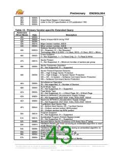
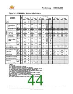
Table 14-1. EN29GL064 Command Definitions
Bus Cycles
Command
Sequence
1st
Addr
P
Cycle
2nd
P
Cycle
3rd
P
Cycle
4th
P
Cycle
5th
Addr Data
P
Cycle
6th
Addr
P
Cycle
Data
P
P
P
P
P
P
Data Addr
Data Addr
Data Addr Data
Read
Reset
1
1
RA
RD
XXX
555
F0
000
100
000
200
7F
Word
Byte
2AA
AA
555
55
Manufacturer
ID
1C
7F
1C
4
90
AAA
555
AAA
Device ID
Uniform
Word
Byte
555
AAA
2AA
AA
555
AAA
X01 227E X0E 220C
7E
X0F
X1E
2201
01
4
4
55
55
90
90
555
X02
X01 227E X0E 2210
7E
X1C
0C
Device ID
Top Boot
Word
555
2AA
AA
555
X0F
2201
Byte
Word
Byte
AAA
555
555
AAA
555
X02
X1C
10
X1E
X0F
X1E
01
2200
00
2AA
AA
X01 227E X0E 2210
Device ID
Bottom Boot
4
4
4
55
55
90
90
7E
00
01
00
01
AAA
555
AAA
X02
X1C
10
(SA)
X02
(SA)
X04
Word
Byte
555
2AA
AA
555
Sector Protect
Verify
AAA
555
AAA
Word
Byte
555
AAA
555
SA
2AA
AA
555
AAA
SA
Program
Write to Buffer
55
55
A0
25
PA
SA
PD
555
WBL
6
1
3
AA
29
2AA
WC
PA
PD
PD
Program Buffer to Flash
Write to Buffer Abort Reset
555
555
AA
2AA
2AA
55
55
555
555
F0
80
Word
555
2AA
555
Chip Erase
6
6
AA
AA
AA
AA
55
55
10
30
Byte
Word
Byte
AAA
555
AAA
555
2AA
555
AAA
555
AAA
AAA
555
AAA
555
2AA
555
AAA
Sector Erase
55
80
SA
Sector Erase Suspend
Sector Erase Resume
1
1
XXX
B0
30
XXX
55
Word
Byte
CFI Query
1
2
98
A0
AA
XX
Accelerated Program
PA
PD
Legend
X = Don’t care
RA = Address of the memory to be read.
RD = Data read from location RA during read operation.
PA = Address of the memory location to be programmed. Addresses latch on
the falling edge of the WE# or CE# pulse, whichever happens later.
PD = Data to be programmed at location PA. Data latches on the rising edge
of the WE# or CE# pulse, whichever happens first.
SA = Address of the sector to be verified (in autoselect mode) or erased.
Address bits Amax–A16 uniquely select any sector.
WBL = Write Buffer Location. The address must be within the same write
buffer page as PA.
WC = Word Count is the number of write buffer locations to load minus 1.
This Data Sheet may be revised by subsequent versions
or modifications due to changes in technical specifications.
©2004 Eon Silicon Solution, Inc., www.eonssi.com
44
Rev. A, Issue Date: 2009/3/20

 EON [ EON SILICON SOLUTION INC. ]