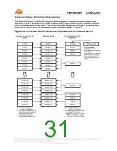
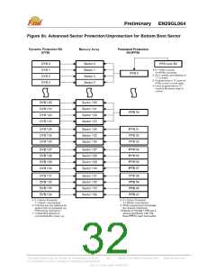
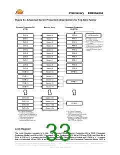
Preliminary EN29GL064
DQ3: Sector Erase Timeout State Indicator
After writing a sector erase command sequence, the output on DQ3 can be checked to determine
whether or not an erase operation has begun. (The sector erase timer does not apply to the chip erase
command.) When sector erase starts, DQ3 switches from “0” to “1”. This device does not support
multiple sector erase (continuous sector erase) command sequences so it is not very meaningful since
it immediately shows as a “1” after the first 30h command. Future devices may support this feature.
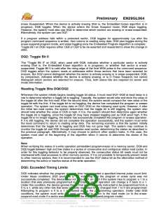
DQ1: Write to Buffer Abort
DQ1 indicates whether a Write to Buffer operation was aborted. Under these conditions DQ1 produces
a “1”. The system must issue the “Write to Buffer Abort Reset” command sequence to return the device
to reading array data.
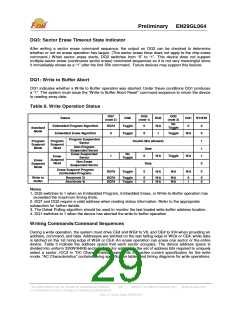
Table 6. Write Operation Status
DQ7
(note 2)
DQ5
(note 1)
DQ2
(note 2)
Status
DQ6
DQ3
DQ1 RY/BY#
No
Toggle
Embedded Program Algorithm
Embedded Erase Algorithm
DQ7#
0
Toggle
Toggle
0
0
N/A
1
0
0
0
Standard
Mode
Toggle
N/A
Program Suspended
Program
Suspend
Mode
Program
Sector
Invalid (Not allowed)
Data
1
Suspend
Non-Program
Read
1
1
Suspended Sector
Erase Suspended
No
1
0
N/A
Toggle
N/A
N/A
N/A
Erase
Suspend
Sector
Toggle
Erase
Suspend
Mode
Non-Erase
Read
Data
0
0
Suspended Sector
Erase Suspend Program
(Embedded Program)
DQ7#
Toggle
0
N/A
Write to
Buffer
Busy(note 3)
Abort(note 4)
DQ7#
DQ7#
Toggle
Toggle
0
0
N/A
N/A
N/A
N/A
0
1
0
0
Notes
1. DQ5 switches to 1 when an Embedded Program, Embedded Erase, or Write-to-Buffer operation has
exceeded the maximum timing limits.
2. DQ7 and DQ2 require a valid address when reading status information. Refer to the appropriate
subsection for further details.
3. The Data# Polling algorithm should be used to monitor the last loaded write-buffer address location.
4. DQ1 switches to 1 when the device has aborted the write-to-buffer operation
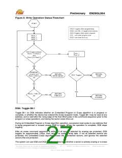
Writing Commands/Command Sequences
During a write operation, the system must drive CE# and WE# to VIL and OE# to VIH when providing an
address, command, and data. Addresses are latched on the last falling edge of WE# or CE#, while data
is latched on the 1st rising edge of WE# or CE#. An erase operation can erase one sector or the entire
device. Table 3 indicate the address space that each sector occupies. The device address space is
divided into uniform 32KW/64KB sectors. A sector address is the set of address bits required to uniquely
select a sector. ICC2 in “DC Characteristics” represents the active current specification for the write
mode. “AC Characteristics” contains timing specification tables and timing diagrams for write operations.
This Data Sheet may be revised by subsequent versions
or modifications due to changes in technical specifications.
©2004 Eon Silicon Solution, Inc., www.eonssi.com
29
Rev. A, Issue Date: 2009/3/20

 EON [ EON SILICON SOLUTION INC. ]