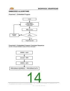
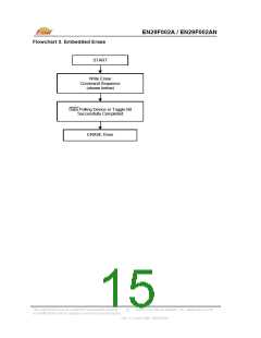
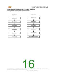
EN29F002A / EN29F002AN
DATA PROTECTION
Power-up Write Inhibit
During power-up, the device automatically resets to READ mode and locks out write cycles. Even
with
W E
= V ,
= VIL and
= VIH, the device will not accept commands on the rising edge of
OE
CE
.
WE
IL
Low VCC Write Inhibit
During VCC power-up or power-down, the EN29F002A locks out write cycles to protect against any
unintentional writes. If VCC < VLKO, the command register is disabled and all internal program or
erase circuits are disabled. Under this condition, the device will reset to the READ mode.
Subsequent writes will be ignored until VCC > VLKO.
Write “Noise” Pulse Protection
Noise pulses less than 5ns on
command register.
,
or
will neither initiate a write cycle nor change the
WE
OE CE
Logical Inhibit
If
=V or
=V , writing is inhibited. To initiate a write cycle,
and
must be a logical
W E
CE
WE
,
CE
are all logical zero (not recommended usage), it will be considered a
IH
IH
“zero”. If
, and
CE
OE
W E
write.
Sector Protection/Unprotection
When the device is shipped, all sectors are unprotected. Each sector can be separately protected
against data changes. Using hardware protection circuitry enabled at user’s site with external
programming equipment, both program and erase operations may be disabled for any specified
sector or combination of sectors.
Verification of write protection for a specific sector can be achieved with an Auto Select ID read
command at location 02h where the address bits A17 - A13 select the defined sector (see Table 5).
A logical “1” at DQ0 means a protected sector and a logical “0” means an unprotected sector.
The Sector Unprotect disables sector protection in all sectors in one operation to implement code
changes. All sectors must be placed in protection mode using the protection algorithm mentioned
above before unprotection can be executed.
Additional details on this feature are provided in a supplement, which can be obtained by contacting
a representative of Eon Silicon Solution, Inc.
This Data Sheet may be revised by subsequent versions
or modifications due to changes in technical specifications.
©2003 Eon Silicon Solution, Inc., www.essi.com.tw
13
Rev. A, Issue Date: 2003/03/26

 EON [ EON SILICON SOLUTION INC. ]