EN25QH32
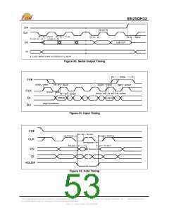
Table 14. AC Characteristics
(Ta = - 40°C to 85°C; VCC = 2.7-3.6V)
Symbol
Alt
Parameter
Min
D.C.
Typ
Max
Unit
MHz
Serial Clock Frequency for:
FAST_READ, PP, SE, BE, DP, RES, WREN,
WRDI, WRSR
-
104
FR
fC
Serial Clock Frequency for:
RDSR, RDID, Dual Output Fast Read
D.C.
D.C.
-
-
80
50
MHz
MHz
Serial Clock Frequency for READ, Quad I/O Fast
Read
fR
1
tCH
Serial Clock High Time
4
4
-
-
-
-
-
-
-
-
-
-
-
-
-
-
-
-
ns
ns
1
tCL
Serial Clock Low Time
2
tCLCH
Serial Clock Rise Time (Slew Rate)
Serial Clock Fall Time (Slew Rate)
CS# Active Setup Time (Relative to CLK)
CS# Active Hold Time (Relative to CLK)
CS# Not Active Setup Time (Relative to CLK)
CS# Not Active Hold Time (Relative to CLK)
0.1
0.1
5
V / ns
V / ns
ns
2
tCHCL
tSLCH
tCHSH
tSHCH
tCHSL
tCSS
5
ns
5
ns
5
ns
CS# High Time for read
CS# High Time for program/erase
15
50
ns
ns
tSHSL
tCSH
tDIS
tHO
tDSU
tDH
-
-
2
tSHQZ
Output Disable Time
-
-
-
-
-
6
-
ns
ns
ns
ns
ns
ns
ns
ns
ns
ns
ns
ns
ns
µs
tCLQX
tDVCH
tCHDX
tHLCH
tHHCH
tCHHH
tCHHL
Output Hold Time
0
2
5
5
5
5
5
Data In Setup Time
-
Data In Hold Time
-
HOLD# Low Setup Time ( relative to CLK )
HOLD# High Setup Time ( relative to CLK )
HOLD# Low Hold Time ( relative to CLK )
HOLD# High Hold Time ( relative to CLK )
HOLD# Low to High-Z Output
HOLD# High to Low-Z Output
Output Valid from CLK
2
tHZ
tLZ
tV
tHLQZ
6
6
8
-
2
tHHQX
tCLQV
-
20
100
-
-
-
-
-
3
tWHSL
Write Protect Setup Time before CS# Low
Write Protect Hold Time after CS# High
CS# High to Deep Power-down Mode
3
tSHWL
-
2
tDP
3
CS# High to Standby Mode without Electronic
Signature read
CS# High to Standby Mode with Electronic
Signature read
2
tRES1
-
-
-
-
3
µs
µs
2
tRES2
1.8
tW
Write Status Register Cycle Time
Page Programming Time
Sector Erase Time
-
-
-
-
-
-
15
1.3
0.09
0.5
25
50
5
ms
ms
6
tPP
tSE
tBE
tCE
0.3
2
Block Erase Time
s
50
28
s
Chip Erase Time
WIP = write operation
Software Reset
-
µs
tSR
Latency
WIP = not in write operation
-
-
0
µs
Note: 1. tCH + tCL must be greater than or equal to 1/ fC
2. Value guaranteed by characterization, not 100% tested in production.
3. Only applicable as a constraint for a Write status Register instruction when Status Register Protect Bit is set at 1.
This Data Sheet may be revised by subsequent versions
or modifications due to changes in technical specifications.
©2004 Eon Silicon Solution, Inc., www.eonssi.com
52
Rev. E, Issue Date: 2012/01/30

 EON [ EON SILICON SOLUTION INC. ]