EN25F40
Power-down
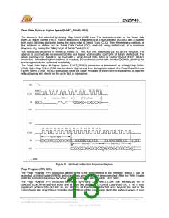
Manufacturer/
Device ID
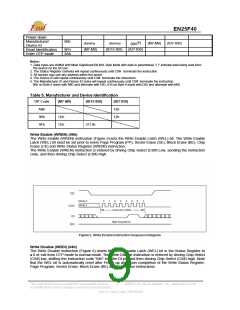
90h
(5)
00h
dummy
dummy
(M7-M0)
(ID7-ID0)
(ID15-ID8)
(ID7-ID0)
(M7-M0)
Read Identification
Enter OTP mode
9Fh
3Ah
Notes:
1. Data bytes are shifted with Most Significant Bit first. Byte fields with data in parenthesis “( )” indicate data being read from
the device on the DO pin.
2. The Status Register contents will repeat continuously until CS# terminate the instruction.
3. All sectors may use any address within the sector.
4. The Device ID will repeat continuously until CS# terminate the instruction.
5. The Manufacturer ID and Device ID bytes will repeat continuously until CS# terminate the instruction.
00h on Byte 4 starts with MID and alternate with DID, 01h on Byte 4 starts with DID and alternate with MID.
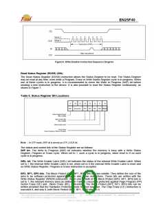
Table 5. Manufacturer and Device Identification
OP Code
(M7-M0)
(ID15-ID0)
(ID7-ID0)
ABh
12h
90h
1Ch
1Ch
12h
9Fh
3113h
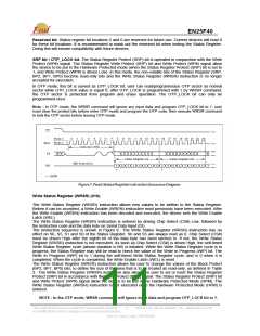
Write Enable (WREN) (06h)
The Write Enable (WREN) instruction (Figure 5) sets the Write Enable Latch (WEL) bit. The Write Enable
Latch (WEL) bit must be set prior to every Page Program (PP), Sector Erase (SE), Block Erase (BE), Chip
Erase (CE) and Write Status Register (WRSR) instruction.
The Write Enable (WREN) instruction is entered by driving Chip Select (CS#) Low, sending the instruction
code, and then driving Chip Select (CS#) High.
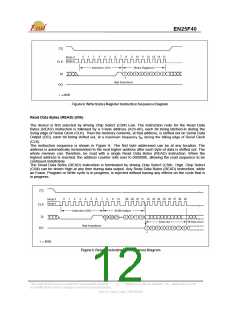
Write Disable (WRDI) (04h)
The Write Disable instruction (Figure 6) resets the Write Enable Latch (WEL) bit in the Status Register to
a 0 or exit from OTP mode to normal mode. The Write Disable instruction is entered by driving Chip Select
(CS#) low, shifting the instruction code “04h” into the DI pin and then driving Chip Select (CS#) high. Note
that the WEL bit is automatically reset after Power-up and upon completion of the Write Status Register,
Page Program, Sector Erase, Block Erase (BE) and Chip Erase instructions.
This Data Sheet may be revised by subsequent versions
or modifications due to changes in technical specifications.
©2004 Eon Silicon Solution, Inc., www.essi.com.tw
9
Rev. B, Issue Date: 2007/05/09

 EON [ EON SILICON SOLUTION INC. ]