EN25F40
Read Data Bytes at Higher Speed (FAST_READ) (0Bh)
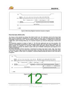
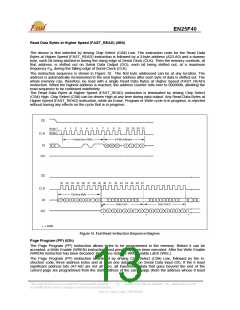
The device is first selected by driving Chip Select (CS#) Low. The instruction code for the Read Data
Bytes at Higher Speed (FAST_READ) instruction is followed by a 3-byte address (A23-A0) and a dummy
byte, each bit being latched-in during the rising edge of Serial Clock (CLK). Then the memory contents, at
that address, is shifted out on Serial Data Output (DO), each bit being shifted out, at a maximum
frequency F , during the falling edge of Serial Clock (CLK).
R
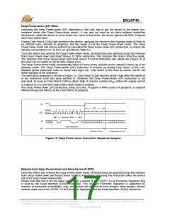
The instruction sequence is shown in Figure 10.. The first byte addressed can be at any location. The
address is automatically incremented to the next higher address after each byte of data is shifted out. The
whole memory can, therefore, be read with a single Read Data Bytes at Higher Speed (FAST_READ)
instruction. When the highest address is reached, the address counter rolls over to 000000h, allowing the
read sequence to be continued indefinitely.
The Read Data Bytes at Higher Speed (FAST_READ) instruction is terminated by driving Chip Select
(CS#) High. Chip Select (CS#) can be driven High at any time during data output. Any Read Data Bytes at
Higher Speed (FAST_READ) instruction, while an Erase, Program or Write cycle is in progress, is rejected
without having any effects on the cycle that is in progress.
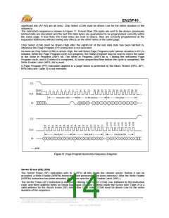
Page Program (PP) (02h)
The Page Program (PP) instruction allows bytes to be programmed in the memory. Before it can be
accepted, a Write Enable (WREN) instruction must previously have been executed. After the Write Enable
(WREN) instruction has been decoded, the device sets the Write Enable Latch (WEL).
The Page Program (PP) instruction is entered by driving Chip Select (CS#) Low, followed by the in-
struction code, three address bytes and at least one data byte on Serial Data Input (DI). If the 8 least
significant address bits (A7-A0) are not all zero, all transmitted data that goes beyond the end of the
current page are programmed from the start address of the same page (from the address whose 8 least
This Data Sheet may be revised by subsequent versions
or modifications due to changes in technical specifications.
©2004 Eon Silicon Solution, Inc., www.essi.com.tw
13
Rev. B, Issue Date: 2007/05/09

 EON [ EON SILICON SOLUTION INC. ]