EN25F40
INSTRUCTIONS
All instructions, addresses and data are shifted in and out of the device, most significant bit first. Serial
Data Input (DI) is sampled on the first rising edge of Serial Clock (CLK) after Chip Select (CS#) is driven
Low. Then, the one-byte instruction code must be shifted in to the device, most significant bit first, on
Serial Data Input (DI), each bit being latched on the rising edges of Serial Clock (CLK).
The instruction set is listed in Table 4. Every instruction sequence starts with a one-byte instruction code.
Depending on the instruction, this might be followed by address bytes, or by data bytes, or by both or
none. Chip Select (CS#) must be driven High after the last bit of the instruction sequence has been shifted
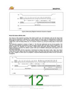
in. In the case of a Read Data Bytes (READ), Read Data Bytes at Higher Speed (Fast_Read), Read
Status Register (RDSR) or Release from Deep Power-down, and Read Device ID (RDI) instruction, the
shifted-in instruction sequence is followed by a data-out sequence. Chip Select (CS#) can be driven High
after any bit of the data-out sequence is being shifted out.
In the case of a Page Program (PP), Sector Erase (SE), Block Erase (BE), Chip Erase (CE), Write Status
Register (WRSR), Write Enable (WREN), Write Disable (WRDI) or Deep Power-down (DP) instruction,
Chip Select (CS#) must be driven High exactly at a byte boundary, otherwise the instruction is rejected,
and is not executed. That is, Chip Select (CS#) must driven High when the number of clock pulses after
Chip Select (CS#) being driven Low is an exact multiple of eight. For Page Program, if at any time the
input byte is not a full byte, nothing will happen and WEL will not be reset.
In the case of multi-byte commands of Page Program (PP), and Release from Deep Power Down
(RES ) minimum number of bytes specified has to be given, without which, the command will be
ignored.
In the case of Page Program, if the number of byte after the command is less than 4 (at least 1 data
byte), it will be ignored too. In the case of SE and BE, exact 24-bit address is a must, any less or
more will cause the command to be ignored.
All attempts to access the memory array during a Write Status Register cycle, Program cycle or Erase
cycle are ignored, and the internal Write Status Register cycle, Program cycle or Erase cycle continues
unaffected.
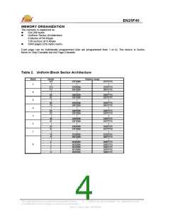
Table 4. Instruction Set
Instruction Name
Byte 1
Code
Byte 2
Byte 3
Byte 4
Byte 5
Byte 6
n-Bytes
Write Enable
06h
04h
Write Disable / Exit
OTP mode
Read Status
Register
continuous
(2)
(1)
05h
(S7-S0)
S7-S0
Write Status
Register
01h
03h
0Bh
A23-A16
A23-A16
A15-A8
A15-A8
A7-A0
A7-A0
(D7-D0)
dummy
D7-D0
(Next byte)
(D7-D0)
Read Data
continuous
(Next Byte)
continuous
Fast Read
Page Program
Sector Erase
Block Erase
02h
20h
A23-A16
A23-A16
A15-A8
A15-A8
A15-A8
A7-A0
A7-A0
A7-A0
(Next byte)
continuous
D8h/ 52h A23-A16
C7h/ 60h
Chip Erase
Deep Power-down
B9h
(4)
Release from Deep
Power-down, and
read Device ID
dummy
ABh
dummy
dummy
(ID7-ID0)
Release from Deep
This Data Sheet may be revised by subsequent versions
or modifications due to changes in technical specifications.
©2004 Eon Silicon Solution, Inc., www.essi.com.tw
8
Rev. B, Issue Date: 2007/05/09

 EON [ EON SILICON SOLUTION INC. ]