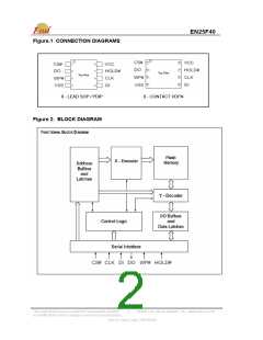
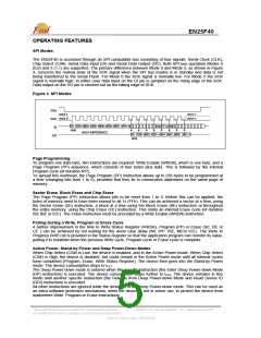
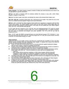
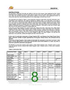
EN25F40
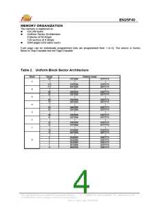
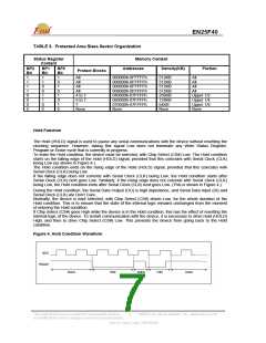
MEMORY ORGANIZATION
The memory is organized as:
z
524,288 bytes
z
Uniform Sector Architecture
8 blocks of 64-Kbyte
128 sectors of 4-Kbyte
2048 pages (256 bytes each)
z
Each page can be individually programmed (bits are programmed from 1 to 0). The device is Sector,
Block or Chip Erasable but not Page Erasable.
Table 2. Uniform Block Sector Architecture
Block
7
Sector
127
Address range
07F000h
07FFFFh
112
111
070000h
06F000h
070FFFh
06FFFFh
6
5
4
3
2
1
96
95
060000h
05F000h
060FFFh
05FFFFh
80
79
050000h
04F000h
050FFFh
04FFFFh
64
63
040000h
03F000h
040FFFh
03FFFFh
48
47
030000h
02F000h
030FFFh
02FFFFh
32
31
020000h
01F000h
020FFFh
01FFFFh
16
15
010000h
00F000h
010FFFh
00FFFFh
4
3
2
1
0
004000h
003000h
002000h
001000h
000000h
004FFFh
003FFFh
002FFFh
001FFFh
000FFFh
0
This Data Sheet may be revised by subsequent versions
or modifications due to changes in technical specifications.
©2004 Eon Silicon Solution, Inc., www.essi.com.tw
4
Rev. B, Issue Date: 2007/05/09

 EON [ EON SILICON SOLUTION INC. ]