EN25F40
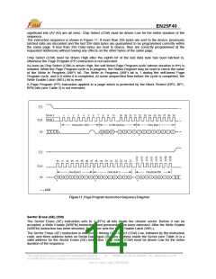
significant bits (A7-A0) are all zero). Chip Select (CS#) must be driven Low for the entire duration of the
sequence.
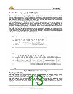
The instruction sequence is shown in Figure 11. If more than 256 bytes are sent to the device, previously
latched data are discarded and the last 256 data bytes are guaranteed to be programmed correctly within
the same page. If less than 256 Data bytes are sent to device, they are correctly programmed at the
requested addresses without having any effects on the other bytes of the same page.
Chip Select (CS#) must be driven High after the eighth bit of the last data byte has been latched in,
otherwise the Page Program (PP) instruction is not executed.
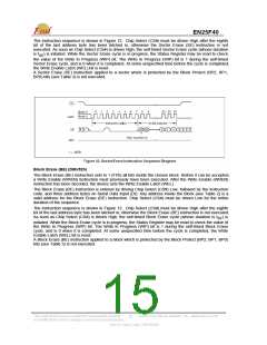
As soon as Chip Select (CS#) is driven High, the self-timed Page Program cycle (whose duration is tPP) is
initiated. While the Page Program cycle is in progress, the Status Register may be read to check the value
of the Write In Progress (WIP) bit. The Write In Progress (WIP) bit is 1 during the self-timed Page
Program cycle, and is 0 when it is completed. At some unspecified time before the cycle is completed, the
Write Enable Latch (WEL) bit is reset.
A Page Program (PP) instruction applied to a page which is protected by the Block Protect (BP2, BP1,
BP0) bits (see Table 3) is not executed.
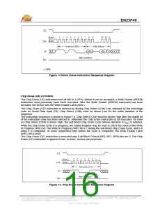
Sector Erase (SE) (20h)
The Sector Erase (SE) instruction sets to 1 (FFh) all bits inside the chosen sector. Before it can be
accepted, a Write Enable (WREN) instruction must previously have been executed. After the Write Enable
(WREN) instruction has been decoded, the device sets the Write Enable Latch (WEL).
The Sector Erase (SE) instruction is entered by driving Chip Select (CS#) Low, followed by the instruction
code, and three address bytes on Serial Data Input (DI). Any address inside the Sector (see Table 2) is a
valid address for the Sector Erase (SE) instruction. Chip Select (CS#) must be driven Low for the entire
duration of the sequence.
This Data Sheet may be revised by subsequent versions
or modifications due to changes in technical specifications.
©2004 Eon Silicon Solution, Inc., www.essi.com.tw
14
Rev. B, Issue Date: 2007/05/09

 EON [ EON SILICON SOLUTION INC. ]