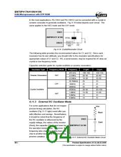
EM78P417N/418N/419N
8-Bit Microprocessor with OTP ROM
6.10.1 External Reference Signal
The analog signal that is presented at Cin– compares to the signal at Cin+, and the
digital output (CO) of the comparator is adjusted accordingly by taking the following
notes into considerations:
NOTE
■ The reference signal must be between Vss and Vdd.
■ The reference voltage can be applied to either pin of comparator.
■ Threshold detector applications may be of the same reference.
■ The comparator can operate from the same or different reference sources.
6.10.2 Comparator Outputs
ꢀ The compared result is stored in the CMPOUT of IOCA0.
ꢀ The comparator outputs are sent to CO(P60) through programming Bit 1,
Bit 0<COS1, COS0> of the IOCA0 register to <1,0>. See Section 6.2.6, IOCA0
(CMPCON: Comparator Control Register) for Comparator/OP select bits function
description.
NOTE
■ The CO and ADEO of the P60/ADE0/CO pins cannot be used at the same time.
■ The P60/ADE0/CO pin priority is as follows:
P60/ADE0/CO PRIORITY
High
CO
Medium
ADE0
Low
P60
The following figure shows the Comparator Output block diagram.
To C0
From OP I/O
CMRD
EN
EN
Q
D
Q
D
To CMPOUT
RESET
To CPIF
CMRD
From other
comparator
Fig. 6-14 Comparator Output Configuration
Product Specification (V1.0) 06.23.2005
• 55
(This specification is subject to change without further notice)

 ELAN [ ELAN MICROELECTRONICS CORP ]