EM78P341N/342N/343N
8-Bit Microprocessor with OTP ROM
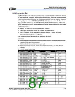
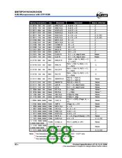
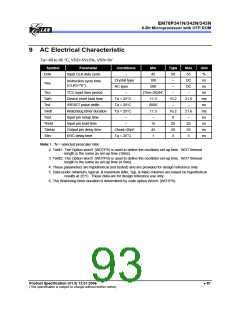
Symbol
Parameter
Offset error
Condition
Min.
Typ.
Max.
Unit
OE
Vdd=VAREF=5.0V, VASS =0.0V
±0
±2
±4
LSB
Recommended
impedance of analog
voltage source
ZAI
–
0
8
10
KΩ
TAD
TCN
ADC clock period
Vdd=VAREF=5.0V, VASS =0.0V
Vdd=VAREF=5.0V, VASS =0.0V
4
–
–
–
us
AD conversion time
15
15
TAD
ADC OP input voltage
range
ADIV
Vdd=VAREF=5.0V, VASS =0.0V
0
–
VAREF
V
V
0
0.2
4.8
0.3
–
0.3
5
ADC OP output voltage
swing
Vdd=VAREF=5.0V, VASS =0.0V,
RL=10KΩ
ADOV
4.7
0.1
±0
ADSR
PSR
ADC OP slew rate
Vdd=VAREF=5.0V, VASS =0.0V
–
V/us
LSB
Power Supply Rejection Vdd=5.0V±0.5V
±2
Note: 1. These parameters are hypothetical (not tested) and are provided for design reference use only.
2. There is no current consumption when ADC is off other than minor leakage current.
3. AD conversion result will not decrease when an increase of input voltage and no missing code will result.
4. These parameters are subject to change without further notice.
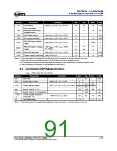
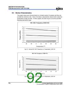
8.2 Comparator (OP) Characteristics
°
Vdd = 5.0V, Vss=0V, Ta=25 C
Symbol
SR
Parameter
Condition
Min.
0.1
0
Typ.
Max.
Unit
V/us
V
Slew rate
0.2
IVR
Input voltage range
Vdd =5.0V, VSS =0.0V
5
0.3
5
0
0.2
4.8
OVS
Output voltage swing
Vd =5.0V, VSS =0.0V, RL=10KΩ
V
4.7
250
Iop
Ico
Supply current of OP
350
300
500
uA
uA
Supply current of Comparator
PSR
R
Power-supply Rejection
Ration for OP
Vdd= 5.0V, VSS =0.0V
50
60
70
dB
V
Vs
Operating range
2.5
5.5
Note: 1. These parameters are hypothetical (not tested) and are provided for design reference use only.
Product Specification (V1.0) 12.01.2006
(This specification is subject to change without further notice)
• 85

 ELAN [ ELAN MICROELECTRONICS CORP ]